Doped graphene, method of manufacturing the doped graphene, and a device including the doped graphene

a technology of doped graphene and manufacturing method, which is applied in the direction of non-metal conductors, conductors, metal/alloy conductors, etc., can solve the problems of difficult separation of single-walled carbon nanotubes, and high cost of carbon nanotube products

Active Publication Date: 2011-06-02
SAMSUNG ELECTRONICS CO LTD
View PDF15 Cites 55 Cited by
  • Summary
  • Abstract
  • Description
  • Claims
  • Application Information

AI Technical Summary

Benefits of technology

[0016]The organic dopant may include at least one n-dopant selected from the group consisting of a reduction product of a substituted or unsubstituted nicotinamide; a reduction product of a compound whi...

Problems solved by technology

Also, it is advantageous to use graphene sheets because products made from graphite may be inexpensive, while products made from carbon nanotubes, which are similar to graphene sheets, may be expensive ...

Method used


Image

  • Doped graphene, method of manufacturing the doped graphene, and a device including the doped graphene
  • Doped graphene, method of manufacturing the doped graphene, and a device including the doped graphene
  • Doped graphene, method of manufacturing the doped graphene, and a device including the doped graphene

Examples


preparation example 1

Preparation of Graphene

[0076]Ni was deposited on a 1.2 centimeter (cm) by 1.5 cm silicon substrate on which 100 nm of SiO2 was coated using sputtering to form a Ni thin film. The silicon substrate on which the SiO2 and the Ni thin film are formed was disposed in a chamber. Then, the silicon substrate was heat-treated at 400° C. for 20 minutes using a halogen lamp to form graphene on the graphitizing catalyst while uniformly adding acetylene gas to the chamber at 200 standard cubic centimeters per minute (sccm).

[0077]Then, the heat source was removed, and the chamber was naturally cooled to grow the graphene in a uniform alignment to form a 1.2 cm by 1.5 cm graphene sheet with 10 layers.

[0078]Then, a chlorobenzene solution (5 weight percent, wt %) in which poly(methyl methacrylate) (“PMMA”) was dissolved was coated on the substrate on which the graphene sheet is formed at 1000 revolutions per minute (“rpm”) for 60 seconds. The resultant was immersed in 0.1 M HNO3 for 1 hour to remove...

example 1

Doping of Graphene

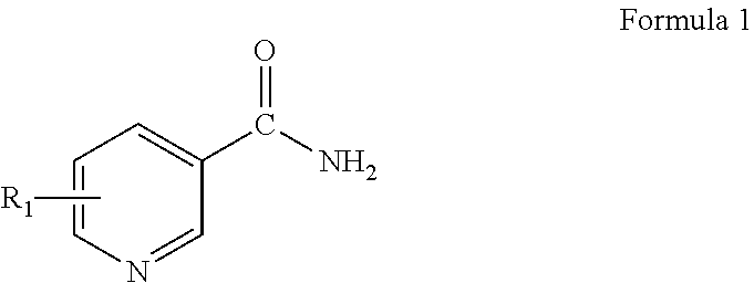
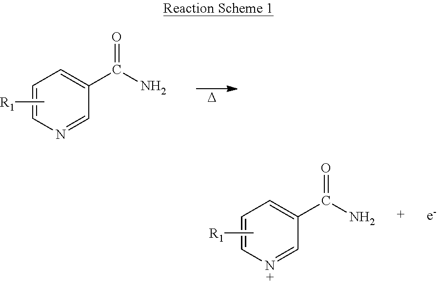
[0079]Graphene sheet films having a transparency up to 72% at 550 nanometers (nm) and prepared according to Preparation Example 1 were respectively immersed in a AuCl3 solution (10 millimolar, mM) as a p-dopant, a dichlorodicyanoquinone (“DDQ”) solution (10 mM) as a p-dopant, and a 1,1′-dibenzyl-4,4′-bipyridinium dichloride (“BV”) solution (10 mM) as a n-dopant, for 1 hour, and then washed with water and dried by spin coating.

experimental example

Identification of Doping Effect of Graphene

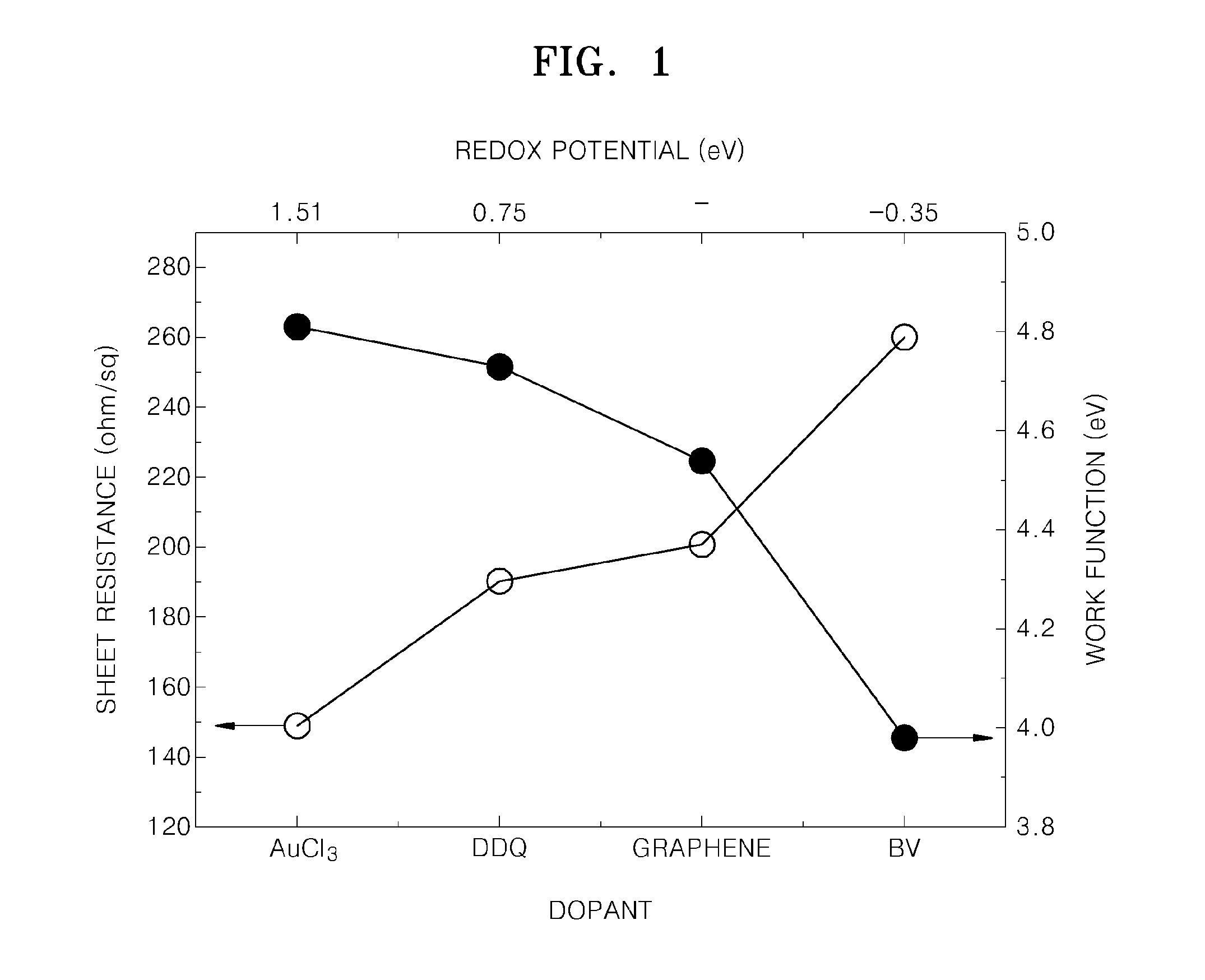
[0080]After doping the graphene, the physical characteristics of graphene were measured. The results are shown in Table 1 below.

TABLE 1DopantConcentration ofRedoxSheetHalldopant inpotentialresistancecoef.grapheneWorkUnitvolts vs SHEohm / sqm2 / C# / cm2functionAuCl31.5114925.92.43E+134.81DDQ0.7519030.62.04E+134.73None—20135.31.77E+134.54(puregraphene)BV−0.35260−29.7−2.10E+13 3.98(SHE refers to standard hydrogen electrode, eV refers to electron volts, ohm / sq refers to ohms per square)

[0081]The redox potential refers to the standard redox potential of each material for comparison with that of the graphene. The sheet resistance was measured using a 4-probe sheet resistivity measurement unit.

[0082]Referring to Table 1, the work function increased as the redox potential increased from negative (−) to positive (+). As shown in Table 1, the work function increased from 3.98 to 4.81. This indicates that the doped graphene may replace a metal electrode su...


PUM


Abstract

A composition including graphene; and a dopant selected from the group consisting of an organic dopant, an inorganic dopant, and a combination including at least one of the foregoing.

Description

CROSS-REFERENCE TO RELATED APPLICATION[0001]This application claims priority to Korean Patent Application No. 10-2009-0118450, filed on Dec. 2, 2009, and all the benefits accruing therefrom under 35 U.S.C. §119, the content of which in its entirety is herein incorporated by reference.BACKGROUND[0002]1. Field[0003]The present disclosure relates to a doped graphene, a method of manufacturing the doped graphene, and an electrode, a display device, and a solar cell including the doped graphene. The doped graphene may have excellent electrical characteristics.[0004]2. Description of the Related Art[0005]Generally, graphite has a structure in which two-dimensional (2D) graphene sheets, in which carbon atoms are connected to each other in a hexagonal array, are stacked on each other. Recently, several studies showed that single-layered or multiple-layered graphene sheets have amazing properties. One notable property is that electrons flow in a graphene sheet as if they are weightless, whic...

Claims


Application Information

Patent Timeline
IPC IPC(8): H01B1/02H01B1/04H01B1/12
CPCB82Y30/00B82Y40/00C01B31/0446H01L51/002H01B1/04H01L29/1606H01L29/167C01B31/0484C01B32/184C01B32/194Y02E10/549H10K71/30
Inventor SHIN, HYEON-JINCHOI, WON-MOOKCHOI, JAE-YOUNGYOON, SEON-MI
Owner SAMSUNG ELECTRONICS CO LTD
Why Eureka
Try Eureka