Compound semiconductor device and method of manufacturing compound semiconductor device

Active Publication Date: 2011-06-02
TOYODA GOSEI CO LTD
View PDF6 Cites 36 Cited by
  • Summary
  • Abstract
  • Description
  • Claims
  • Application Information

AI Technical Summary

Benefits of technology

[0027]In the method of manufacturing a compound semiconductor device according to the present invention, the division step includes a first division step of dividing the wafer in the first direction to obtain first strip wafers each having at least two rows of the device portions arranged in the first direction; a second division step of dividing the first strip wafer in the second direction to obtain second strip wafers each having a row of the device portions arranged in the second direction; and a third division step of dividing the second strip wafer into the device portions, thereby forming the compound semiconductor devices including the device portions. Therefore, it is possible to reduce the distortion of the substrate when the wafer is divided in the second direction, which will be described below, as compared to when the wafer is divided into strip-shaped device blocks, each having a row of device portions arranged in the first direction.
[0028]That is, in the present invention, the first strip wafer divided in the second division step has at least two

Problems solved by technology

However, when a semiconductor light-emitting device having an epitaxial layer made of a group-III nitride semiconductor formed on a sapphire substrate is manufactured, a large distortion occurs in the interface between the group-III nitride semiconductor layer and the sapphire substrate due to a large difference between the lattice constants of the group-III nitride semiconductor layer and the sapphire substrate.
Therefore, it is difficult to divide the sapphire su

Method used


Image

  • Compound semiconductor device and method of manufacturing compound semiconductor device
  • Compound semiconductor device and method of manufacturing compound semiconductor device
  • Compound semiconductor device and method of manufacturing compound semiconductor device

Examples


example 1

[0109]As a compound semiconductor device, a group-III nitride semiconductor light-emitting device including the LED device structure having a gallium nitride compound semiconductor was manufactured as follows. First, a plurality of LED device structures were formed on the main surface of a substrate, thereby manufacturing a wafer.

(Device Forming Process)

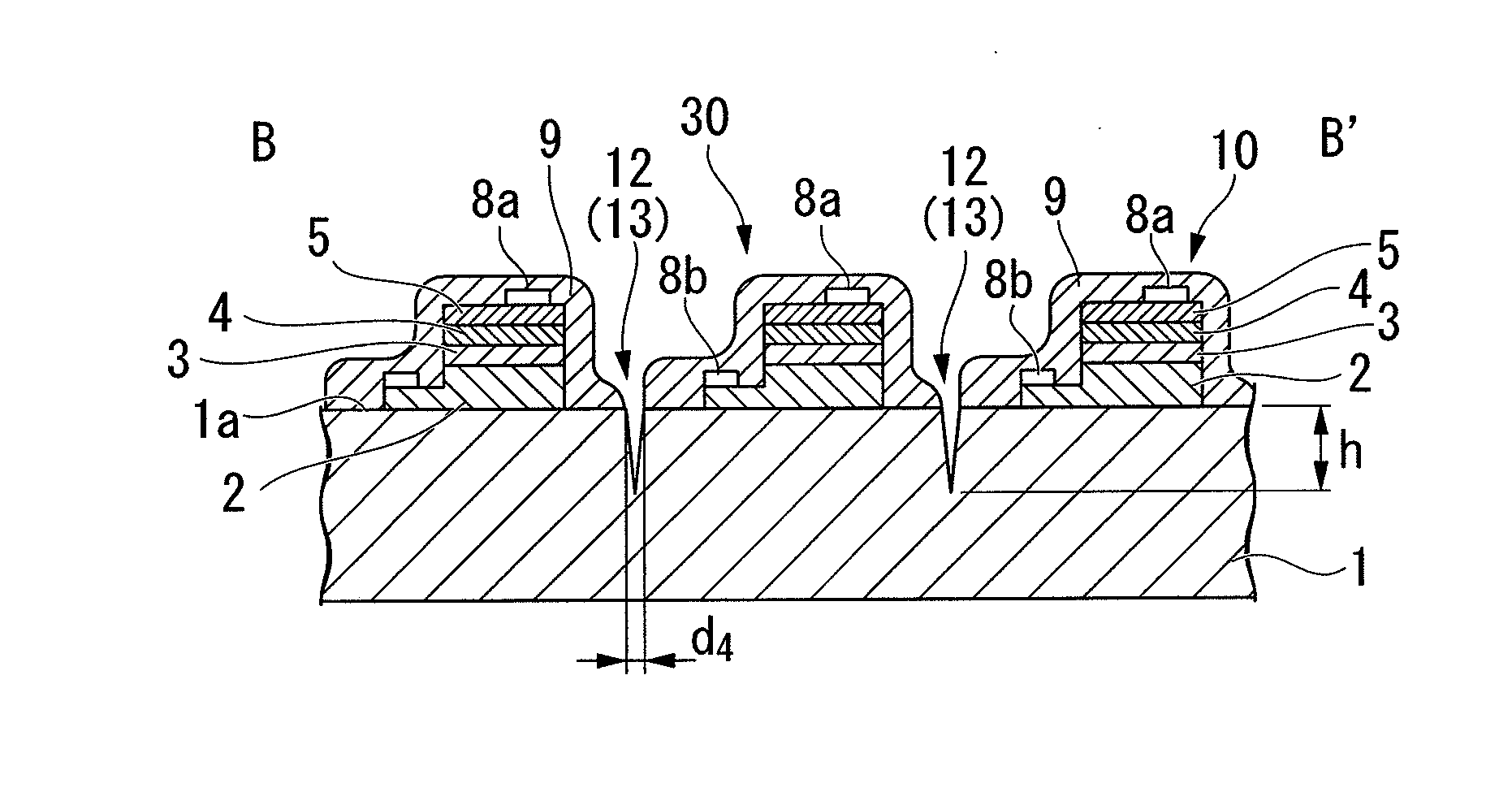
[0110]An epitaxial layer that was made of a group-III nitride semiconductor and had a thickness of 9 μm was manufactured by sequentially laminating, on the main surface of a C-plane sapphire substrate having an outside diameter of 250 μm, an undoped GaN underlying layer with a thickness of 4 μm, a Si-doped (concentration=1×10¹⁹ / cm3) n-type GaN contact layer with a thickness of 2 μm, a Si-doped (concentration=1×10¹⁸ / cm3) n-type In0.1Ga0.9N clad layer with a thickness of 12.5 nm, a light-emitting layer having a multiple quantum well structure, a Mg-doped (concentration=1×10²⁰ / cm3) p-type Al0.07Ga0.93N clad layer with a thickness of 2.5...

example 6

[0129]The same partition process as that in Example 1 was performed on the wafer obtained by the same method as that in Example 1. Then, the division process was performed.

[0130]Cracks occurred in the wafer are shown in FIG. 6. FIG. 6 is a photograph showing the cracks occurred in the wafer.


PUM

PropertyMeasurementUnit
Thicknessaaaaaaaaaa
Thicknessaaaaaaaaaa

Abstract

The present invention provides a method of manufacturing a compound semiconductor device capable of improving yield when a wafer is divided into device regions. The method of manufacturing a compound semiconductor device includes a division step. The division step includes: a first division step of dividing a wafer 30 in a first direction α to obtain first strip wafers each having at least two rows of device portions 10 arranged in the first direction α; a second division step of dividing the first strip wafer in a second direction β to obtain second strip wafers each having a row of the device portions 10 arranged in the second direction β; and a third division step of dividing the second strip wafer into the device portions 10, thereby forming compound semiconductor devices including the device portions 10.

Description

TECHNICAL FIELD[0001]The present invention relates to a compound semiconductor device and a method of manufacturing a compound semiconductor device, and more particularly, to a method of manufacturing a compound semiconductor device capable of improving yield when a wafer is divided into device portions to form compound semiconductor devices and to a compound semiconductor device manufactured by the manufacturing method.[0002]Priority is claimed on Japanese Patent Application No. 2007-033523, filed Feb. 14, 2007, the content of which is incorporated herein by reference.BACKGROUND ART[0003]In recent years, a semiconductor light-emitting device, such as a p-n junction light-emitting diode (LED) or a laser diode (LD), has been known as a compound semiconductor device. In the light-emitting device, when a group-III nitride semiconductor (AlxGayInzN: 0≦x≦1, 0≦y≦1, 0≦z≦1, and x+y+z=1) is used for a light-emitting layer, it is possible to obtain a light-emitting device that emits near ultr...

Claims


Application Information

Patent Timeline
IPC IPC(8): H01S5/00H01L21/78H01L33/00H01L33/06H01L33/32
CPCB23K26/4075H01L33/0095H01L21/78B23K2201/40B23K26/40B23K2101/40B23K2103/50
Inventor KATO, KAZUHIRO
Owner TOYODA GOSEI CO LTD
Why Eureka
Try Eureka