Pattern inspection device and method

Inactive Publication Date: 2011-06-09
HITACHI HIGH-TECH CORP
View PDF9 Cites 44 Cited by
  • Summary
  • Abstract
  • Description
  • Claims
  • Application Information

AI Technical Summary

Benefits of technology

[0025]According to this invention, it is possible to suppress the electron beam's focus drift and irradiation position deviation which are caused by the charge-up phenomenon on a sample surface occurring due to electron

Problems solved by technology

In these fabrication processes, the quality of a fabrication processing result and the generation of particles greatly affect the yield of semiconductor devices.
However, since the resolution of such inspection device depends upon the wavelength of light, it becomes unable to cope with the trend of miniaturization of patterns, resulting in restriction of the application thereof.
While a semiconductor wafer which is different per inspection is mounted by either manpower or machine conveyance on a sample support table that is provided in the inspection device, the wafer's setting position with respect to the sample table does not become constant in a strict sense due to the presence of a conveyance error.
However, in real semiconductor wafers, the pattern layout is different on a per-product basis; so, the alignment mark position is disparate, causing deviation to take place in the correction value of the rotatio

Method used


Image

  • Pattern inspection device and method
  • Pattern inspection device and method
  • Pattern inspection device and method

Examples


embodiment 1

[0051]One embodiment of his invention will now be explained below with reference to the drawings.

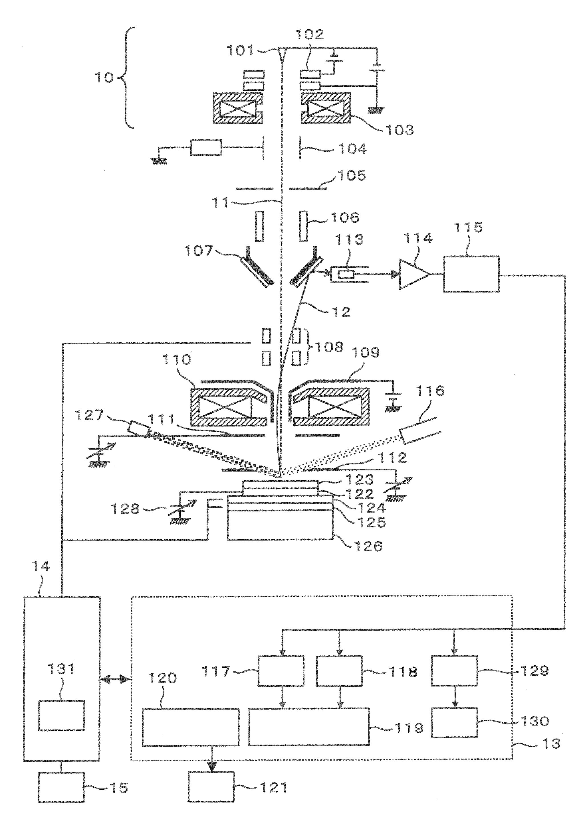
[0052]FIG. 1 is a longitudinal cross-sectional diagram showing a configuration of main part of a semiconductor wafer inspection apparatus using an electron beam, wherein the illustration of a vacuum vessel is omitted. The inspection apparatus of this embodiment is generally made up of an electron optical column which irradiates a primary electron beam onto a sample, detects secondary particles generated, and then outputs a detection result as a secondary signal; X-stage and Y-stage for moving in an X-Y plane a sample table that mounts the above-mentioned sample thereon; an image processing unit 13 which executes prespecified calculation processing to the above-mentioned secondary signal; and a control unit 14 which controls respective devices or equipments of the inspection apparatus, such as the above-noted electron optical column, the X-stage 124 or the Y-stage 125, and others.

[0053]Al...

embodiment 2

[0087]While in the embodiment 1 the inspection device has been explained which is arranged to calculate the position shift and focus shift correction values at the inspection recipe setup stage prior to execution of the inspection, an explanation will be given of an embodiment that is arranged to control the primary electron beam's scan region(s) and irradiation condition(s) while calculating the position shift and focus shift correction values in executing wafer inspection in this embodiment.

[0088]Although no extreme position shift or focus shift is supposed to take place in actual inspections when having calculated the position shift and focus shift correction values in the inspection recipe, the actually performed inspection can experience the generation of little position shift or focus shift even if the correction values that were set up in the recipe are used to control the primary electron beam. In other words, although calculating the position shift or focus shift correction...

embodiment 3

[0110]In this embodiment, a modified example of the embodiment 1 will be explained. Entire apparatus configuration and recipe setup flow are almost the same as those of the embodiment 1 and FIG. 1 or FIG. 2 will be arbitrarily used in the explanation below. Additionally, in a similar manner to the embodiment 2, the same explanation as to the reused drawing(s) will not be repeated herein.

[0111]FIG. 19 and FIG. 20 are graphs showing the relationships of semiconductor wafer surface height measurement values measured by a height sensor and focus conditions. FIG. 19 is in the case of a semiconductor wafer at the contact-hole step shown in FIG. 11 or FIG. 12 whereas FIG. 20 is in the case of a semiconductor wafer at the wiring step shown in FIG. 13. They indicate electrical currents of the objective lens at the focusing condition as the focus condition of the vertical axis. When the structure of a semiconductor wafer is easily affected by charge-up, FIG. 19 indicates that the focus can dr...


PUM


Abstract

An inspection apparatus and method are provided capable of suppressing electron beam focus drifts and irradiation-position deviations caused by sample surface charge-up by irradiation of an electron beam during micropattern inspection to thereby avoid false defect detection and also shorten an inspection time. The apparatus captures a plurality of images of alignment marks provided at dies, stores in a storage device deviations between the central coordinates of alignment mark images and the coordinates of the marks as a coordinate correction value, measures heights at a plurality of coordinates on the sample surface, captures images of the measured coordinates to perform focus adjustment, saves the relationship between such adjusted values and the sensor-measured heights in the storage as height correction values, and uses inspection conditions including the image coordinate correction values saved in the storage and the height correction values to correct the image coordinates and height of the sample.

Description

RELATED APPLICATIONS[0001]This application is the U.S. National Phase under 35 U.S.C. §371 of International Application No. PCT / JP2009 / 066464, filed on Sep. 14, 2009, which in turn claims the benefit of Japanese Application No. 2008-235847, filed on Sep. 16, 2008, the disclosures of which applications are incorporated by reference herein.TECHNICAL FIELD[0002]The present invention relates to an inspection apparatus and inspection method for use in fabrication processes of substrates having fine patterns, such as semiconductor devices, lithography masks, and liquid crystal substrates.BACKGROUND ART[0003]Upon explanation of a fine pattern inspection apparatus and method, an explanation will here be given of micro-pattern inspection in the fabrication process of a semiconductor device as one example. Since the same principle is also applicable to lithography masks, liquid crystal display panels, and the like there are no difficulties in application of the invention stated in this exampl...

Claims


Application Information

Patent Timeline
IPC IPC(8): H01J37/26G12B13/00G01N23/22
CPCH01J37/265H01J37/28H01L22/12H01J2237/2817H01J2237/20292
Inventor NOZOE, MARININOMIYA, TAKU
Owner HITACHI HIGH-TECH CORP
Why Eureka
Try Eureka