Electron detection device and scanning electron microscope

a scanning electron microscope and detection device technology, applied in material analysis using wave/particle radiation, instruments, nuclear engineering, etc., can solve the problems of inability to accurately determine, reduce the vacuum inside the device, and inability to accurately calculate the image on the sample surface, etc., to achieve the effect of accurate calculation, easy and accurate determination

Active Publication Date: 2011-06-16
ADVANTEST CORP
View PDF5 Cites 12 Cited by
  • Summary
  • Abstract
  • Description
  • Claims
  • Application Information

AI Technical Summary

Benefits of technology

[0022]In the present invention, the ratio of the detection value of the secondary electrons generated from the position of the sample irradiated with the electron beam is calculated for each of the divided regions. Thereafter, the inclination angle is determined based on the relationship between the ratio of the secondary electron detection value for each divided region and the inclination angle at the irradiation position, which have been previously measured. Since the secondary el

Problems solved by technology

As a result, there is a problem of unstable quality of the image on the sample surface.
However, introduction of the ozone gas or the like lowers a degree of vacuum inside the device.
Thus, in a low vacuum environment, accurate measurement becomes difficult due to contamination o

Method used


Image

  • Electron detection device and scanning electron microscope
  • Electron detection device and scanning electron microscope
  • Electron detection device and scanning electron microscope

Examples


Embodiment Construction

[0030]With reference to the drawings, an embodiment of the present invention will be described below.

(Configuration of Scanning Electron Microscope)

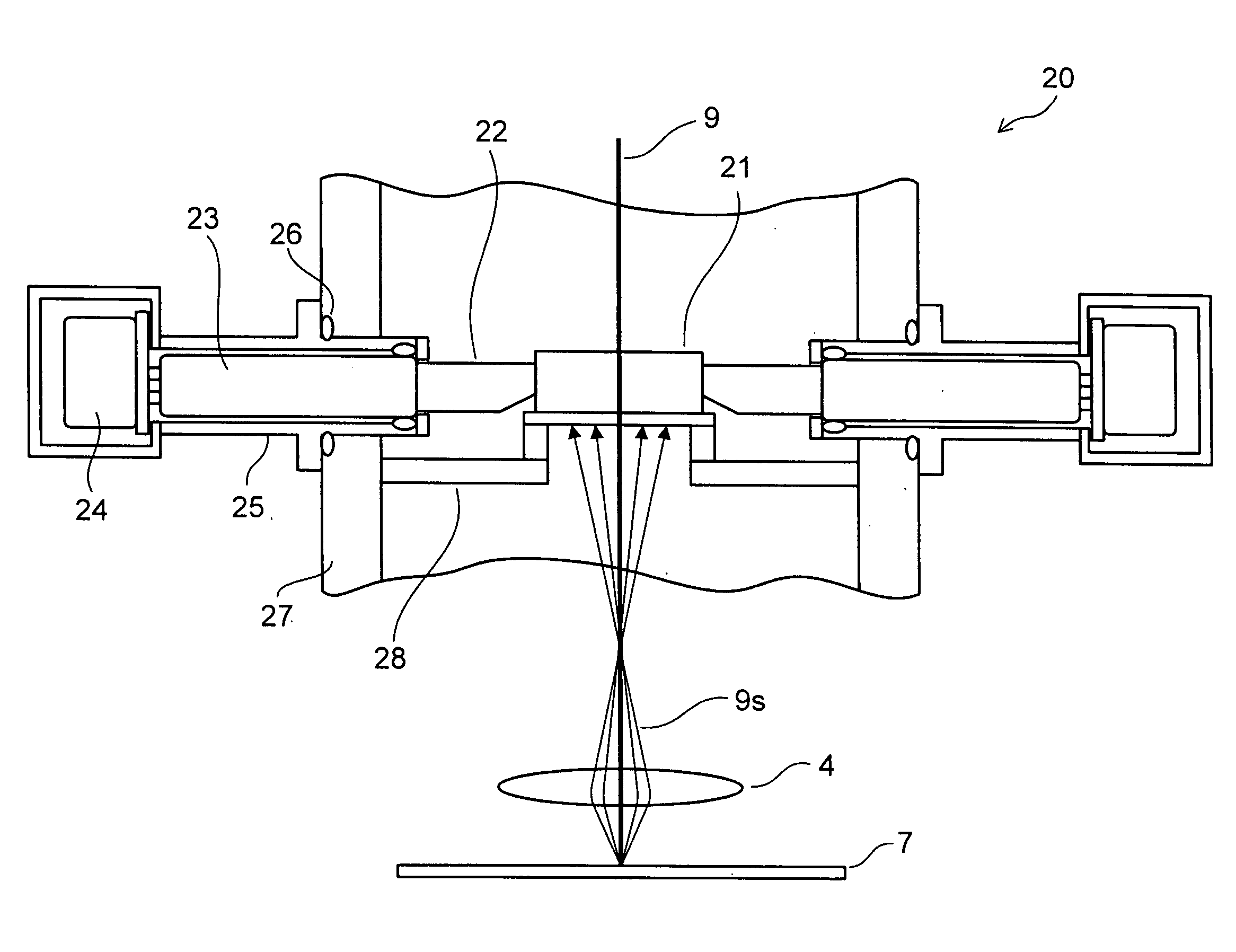
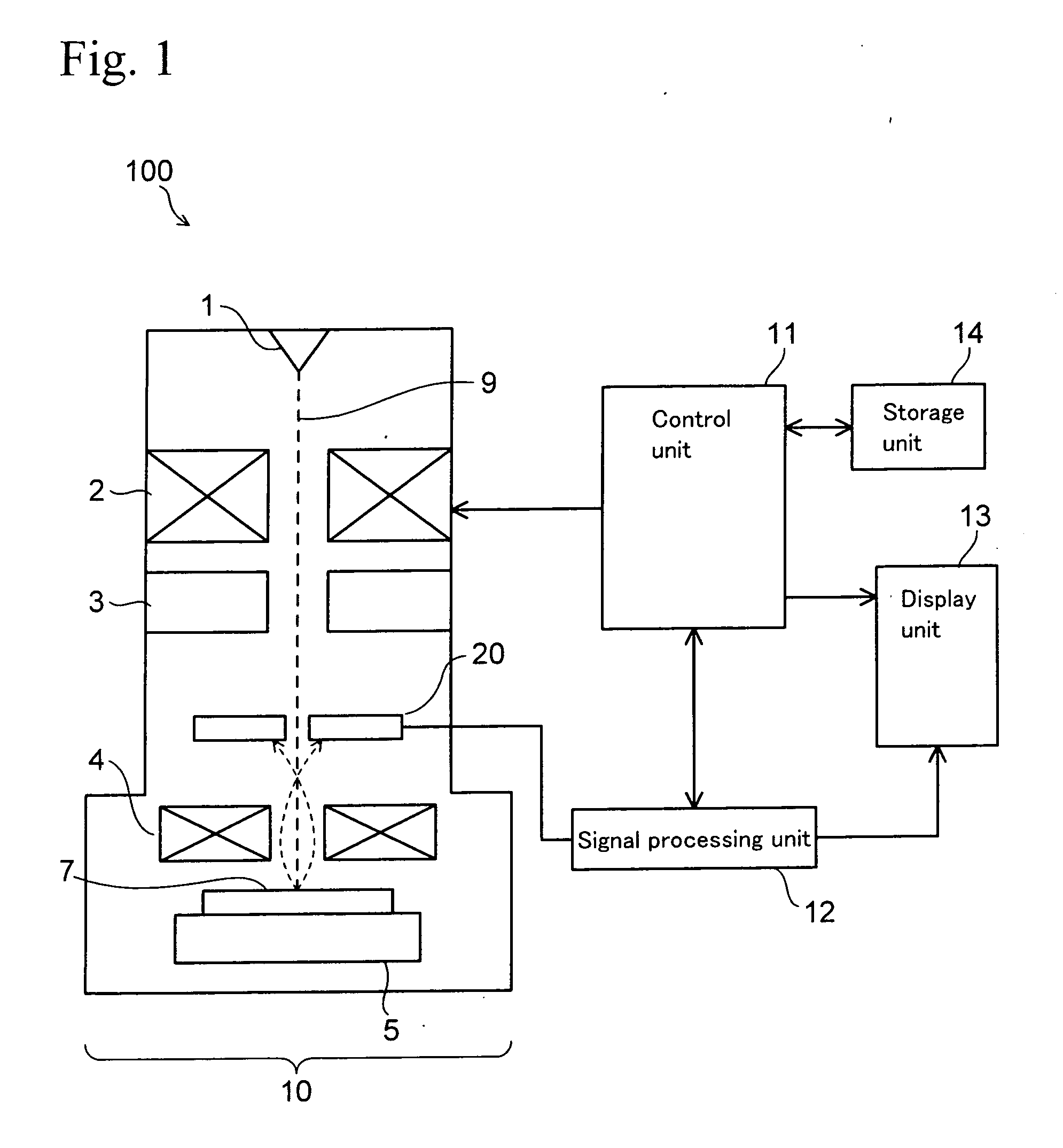
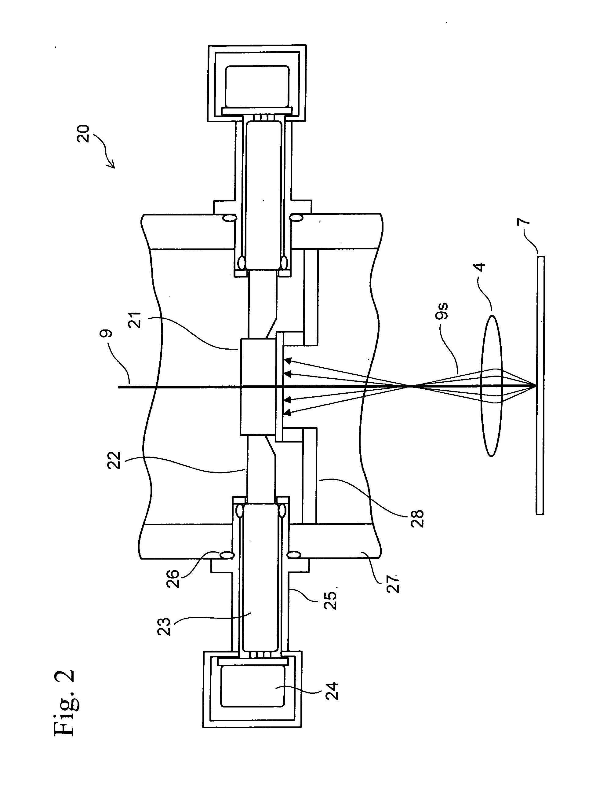
[0031]FIG. 1 is a configuration diagram of a scanning electron microscope 100 according to this embodiment. This scanning electron microscope 100 is mainly composed of an electron lens-barrel unit 10, a signal processing unit 12, a display unit 13, a storage unit 14 and a control unit 11 for controlling the electron lens-barrel unit 10, the signal processing unit 12, the display unit 13 and the storage unit 14.

[0032]The electron lens-barrel unit 10 has an electron gun 1, a condensing lens 2, a deflection coil 3, an objective lens 4 and an electron detector (electron detection device) 20. Moreover, a sample 7 is placed on a stage 5, and a motor (not shown) for moving the stage 5, a vacuum pump (not shown) for maintaining the inside of the electron lens-barrel at a predetermined reduced-pressure atmosphere and a gas introducer (not shown) ...


PUM


Abstract

An electron detection device including: one scintillator 31 having an opening through which an electron beam emitted from an electron gun passes; a plurality of photoguides 22 of the same shape, which are bonded to the scintillator and disposed symmetrically about an optical axis; and a photomultiplier tube which is connected to one side of each of the photoguides 22, the side opposing to the optical axis side, and converts light into electrical signals, the light being emitted by the scintillator 31 receiving light through the photoguide 22. The photoguides 22 are joined so as to equally divide the scintillator 31 symmetrically about the optical axis. Moreover, a position and an area of a portion bonded to the scintillator 31, in each of the photoguides 22, are the same among the photoguides 22.

Description

CROSS-REFERENCE TO THE RELATED APPLICATION[0001]This application is a continuation of prior International Patent Application No. PCT / JP2008 / 02248, filed Aug. 20, 2008, the entire contents of which are incorporated herein by reference.BACKGROUND OF INVENTION[0002]1. Technical Field[0003]The present invention relates to an electron detection device and a scanning electron microscope. More particularly, the present invention relates to an electron detection device and a scanning electron microscope capable of detecting electrons emitted from a sample with high accuracy even in a low vacuum environment.[0004]2. Background Art[0005]In a manufacturing process of a semiconductor device, observation of a sample and measurement of a pattern line width and the like are performed by use of an electron beam device such as an electron microscope. In the observation or the measurement of the sample by use of the electron beam device, a portion to be observed is scanned while being irradiated with...

Claims


Application Information

Patent Timeline
IPC IPC(8): G01N23/225G01T1/20
CPCH01J37/244H01J2237/2814H01J2237/24465H01J2237/2443
Inventor KURATA, TSUGUO
Owner ADVANTEST CORP
Why Eureka
Try Eureka