Thin film transistor, display device, and electronic device

a thin film transistor and display device technology, applied in the direction of transistors, semiconductor devices, electrical apparatus, etc., can solve the problems of insufficient heat resistance of oxide semiconductors, lower resistance of oxide semiconductor layers, and electrically shallow impurity levels, so as to maintain the electrical characteristics of oxide semiconductors and improve reliability.

Active Publication Date: 2011-06-16
JOLED INC
View PDF7 Cites 51 Cited by
  • Summary
  • Abstract
  • Description
  • Claims
  • Application Information

AI Technical Summary

Benefits of technology

[0015]According to the thin film transistor of an embodiment of the invention, the first insulating film (gate insulating film) is provided on the gate electrode side of the oxide semiconductor layer, the second insulating film is provided on the source / drain electrodes side, and the first insulating film and / or the second insulating film contain / contains fluorine. With the configuration, a negative fixed charge is generated in the insulating film containing fluorine, and the threshold voltage is shifted to the positive direction by the negative fixed charge. Even in the case where a lattice defect occurs due to separation of oxygen in the oxide semiconductor layer, the lattice defect is compensated by fluorine. Thus, the electric characteristics of the oxide semiconductor are maintained stably. Therefore, the oxide semiconductor is used as a channel, the threshold voltage is controlled to the positive direction, and reliability is improved.

Problems solved by technology

It is also known that heat resistance of the oxide semiconductor is insufficient, and oxygen, zinc, and the like are separated by heat treatment in a TFT manufacturing process, and a lattice defect is caused.
The lattice defect makes electrically shallow impurity level, and causes lower resistance of an oxide semiconductor layer.
A defect level increases, the threshold voltage decreases, and leak current increases.
There is consequently a disadvantage that the transmission characteristics of a TFT fluctuate in a manufacturing process and the like, and the threshold voltage shifts in a negative (−(minus)) direction.
In such a case, when the threshold voltage becomes a negative value, the circuit configuration becomes complicated and it is undesirable.
In the TFT using the oxide semiconductor, however, a technique for sufficiently improving reliability is not established.

Method used


Image

  • Thin film transistor, display device, and electronic device
  • Thin film transistor, display device, and electronic device
  • Thin film transistor, display device, and electronic device

Examples


first embodiment

Configuration of Thin Film Transistor 1

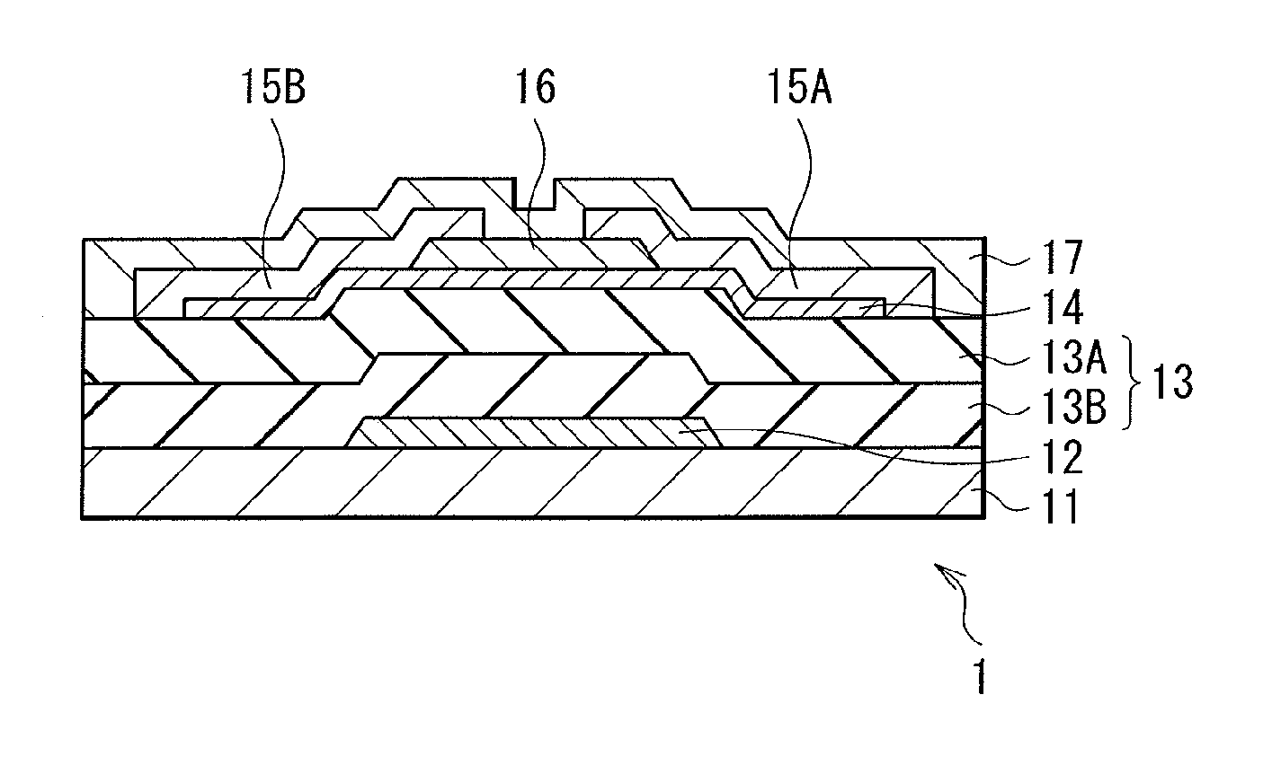
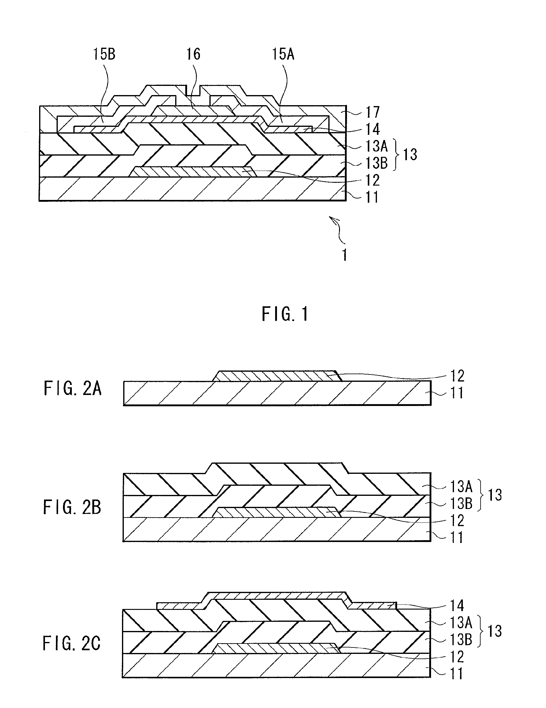
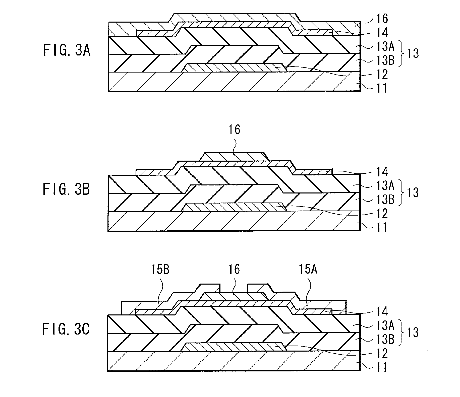
[0041]FIG. 1 illustrates a sectional structure of a thin film transistor 1 according to a first embodiment of the present invention. The thin film transistor 1 is a TFT of a so-called bottom-gate type (inverted staggered structure), in which oxide semiconductor is used for a channel (active layer). In the thin film transistor 1, a gate electrode 12, a gate insulating film 13, an oxide semiconductor layer 14, a channel protection film 16, and source / drain electrodes 15A and 15B are formed in this order on a substrate 11 made of glass or the like. On the source / drain electrodes 15A and 15B, a protection film 17 is formed on the entire face of the substrate 11. The gate insulating film 13 is a concrete example of a “first insulating film” of the invention, and the channel protection film 16 is a concrete example of a “second insulating film” of the invention.

[0042]The gate electrode 12 plays the role of controlling carrier density (in the embodime...

example

[0066]As an example of the foregoing first embodiment, the transmission characteristic (the relation between the gate voltage and the drain current) of the TFT was measured, and a BT test (Bias-Temperature test) was conducted. The transmission characteristics of TFTs in the case where gas containing fluorine was used (example) as a material gas at the time of forming a channel protection film (silicon oxide film) by plasma CVD and those in the case where the gas was not used (comparative example) were measured. FIG. 4 illustrates the results of the measurement. The material gas was adjusted so that the fluorine concentration in the channel protection film in the example becomes 1.0×10²⁰ atom / cm3. It is understood that the transmission characteristic of the TFT shifts to the positive direction by about 2V in the example using the channel protection film formed by using the gas containing fluorine as compared with the comparative example using the channel protection film containing no...

second embodiment

[0083]FIG. 8 illustrates a sectional structure of the thin film transistor 3 according to a second embodiment of the present invention. The thin film transistor 3 is a so-called top-gate (staggered-structure) TFT, in which oxide semiconductor is used for a channel. In the thin film transistor 3, a base coat film 21, the source / drain electrodes 15A and 15B, the oxide semiconductor layer 14, the gate insulating film 13, and the gate electrode 12 are formed in this order on the substrate 11 made of glass or the like. On the gate electrode 12, the protection film 17 is formed on the entire face of the substrate 11. In the embodiment, although the layout of components is different from that of the bottom-gate-type TFT described in the first embodiment, the functions and materials of the components are similar to those of the first embodiment. Therefore, the same reference numerals are designated for convenience, and their description will not be repeated.

[0084]In the embodiment, the base...


PUM


Abstract

The present invention provides a thin film transistor using an oxide semiconductor as a channel, controlling threshold voltage to a positive direction, and realizing improved reliability. The thin film transistor includes: a gate electrode; a pair of source/drain electrodes; an oxide semiconductor layer provided between the gate electrode and the pair of source/drain electrodes and forming a channel; a first insulating film as a gate insulating film provided on the gate electrode side of the oxide semiconductor layer; and a second insulating film provided on the pair of source/drain electrodes side of the oxide semiconductor layer. The first insulating film and/or the second insulating film contain/contains fluorine.

Description

BACKGROUND OF THE INVENTION[0001]1. Field of the Invention[0002]The present invention relates to a thin film transistor using an oxide semiconductor for a channel layer, and a display device and an electronic device each using the thin film transistor.[0003]2. Description of the Related Art[0004]In recent years, with the aim of application of a thin film transistor (TFT), a light emitting device, a transparent conductive film, and the like to electronic devices, research and development on oxide semiconductors such as zinc oxide and indium gallium zinc oxide is actively performed. It is known that, in the case of using such oxide semiconductor to an active layer (channel) of a TFT, as compared with the case of using amorphous silicon which is generally used for a liquid crystal display or the like, the electron mobility is higher, and more excellent electric characteristics are displayed. There are also advantages such that the high mobility is expected even at a low temperature aro...

Claims


Application Information

Patent Timeline
Patent Type & Authority Applications(United States)
IPC IPC(8): H01L29/786
CPCH01L29/4908H01L29/7869H01L29/78606
Inventor MOROSAWA, NARIHIROFUKUMOTO, ERITERAI, YASUHIRO
Owner JOLED INC
Why Eureka
Try Eureka