Delta-doping at wafer level for high throughput, high yield fabrication of silicon imaging arrays

a silicon imaging array and wafer level technology, applied in vacuum evaporation coatings, chemical vapor deposition coatings, coatings, etc., can solve the problems of loss of resolution by absorption, reduction of quantum efficiency, and performance loss of early back-illuminated devices, and achieve the effect of preventing the interaction of minority carriers

Active Publication Date: 2011-06-16
CALIFORNIA INST OF TECH
View PDF8 Cites 28 Cited by
  • Summary
  • Abstract
  • Description
  • Claims
  • Application Information

AI Technical Summary

Benefits of technology

[0008]According to one aspect the invention features a method and apparatus for implementing surface passivation by quantum exclusion, in which subnanometer-scale control over surface structures and materials produces a buried electronic surface that isolates the physical surface from the bulk semiconductor material, and prevents the interaction of minority carriers with surface defects.

Problems solved by technology

In this configuration, structures designed for circuit operation (including patterned oxides, polysilicon electrodes, and metal interconnects) cause reduction of quantum efficiency and loss of resolution by absorption and scattering of incident light.
Back-illuminated detectors were demonstrated as early as 1974, but the performance of these early back-illuminated devices suffered from the lack of an adequate surface passivation technology.

Method used


Image

  • Delta-doping at wafer level for high throughput, high yield fabrication of silicon imaging arrays
  • Delta-doping at wafer level for high throughput, high yield fabrication of silicon imaging arrays
  • Delta-doping at wafer level for high throughput, high yield fabrication of silicon imaging arrays

Examples


Embodiment Construction

Delta Doping

Passivation of Semiconductor Surfaces by Quantum Exclusion

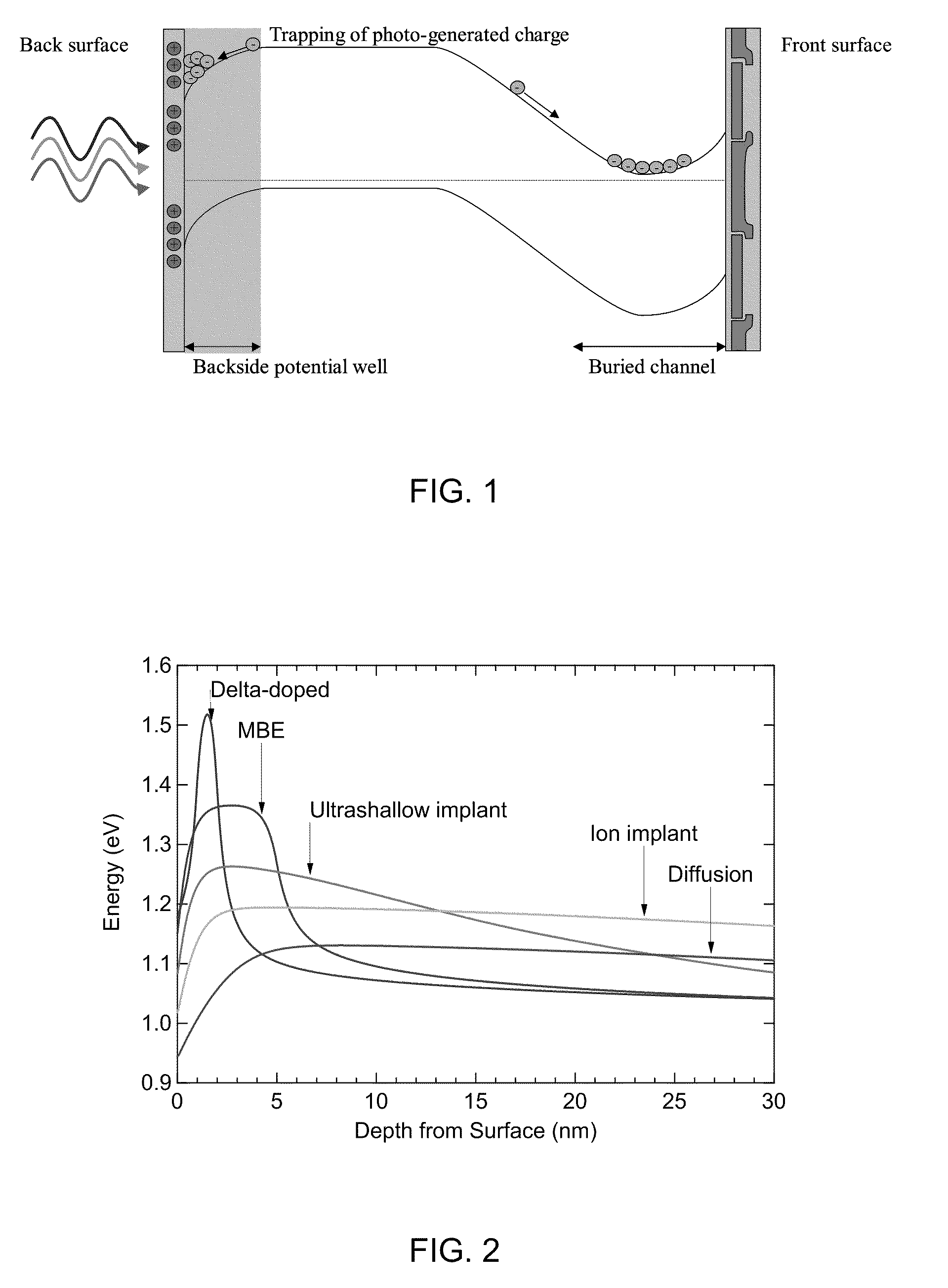
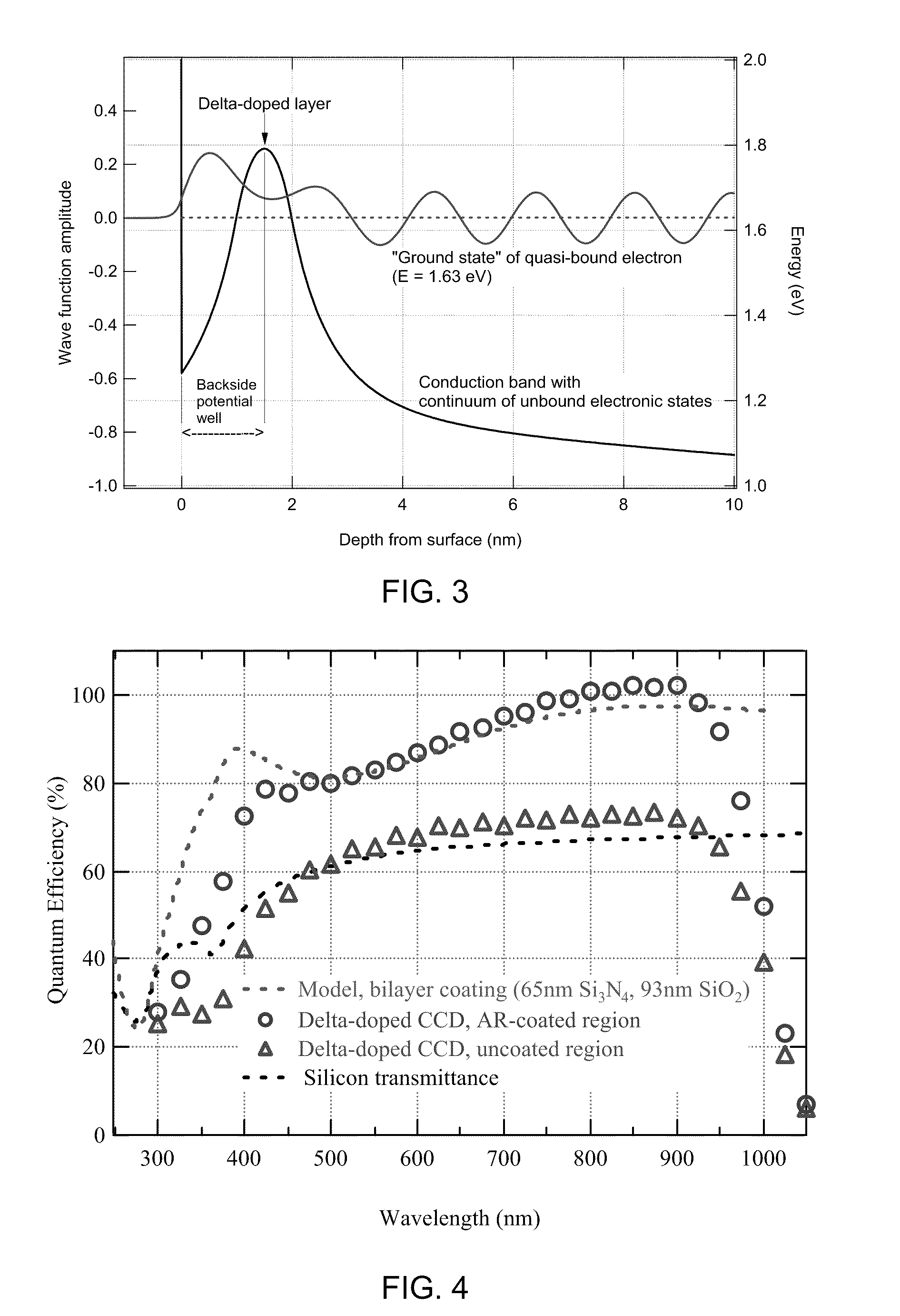
[0072]Growth of highly doped silicon by molecular beam epitaxy, first demonstrated at the Jet Propulsion Laboratory (JPL) in 1991, is the only surface passivation technology that eliminates quantum efficiency hysteresis in back-illuminated scientific imaging arrays. Delta-doping Tests specifically designed to characterize the stability of delta-doped detectors and to search for signs of hysteresis showed no trace of hysteretic response. Quantum exclusion both explains the exceptional performance of delta-doped CCDs, and extends the concepts and applications to existing devices, novel devices, and new applications that are relevant to NASA's conduct of aeronautical and space activities.

[0073]Surfaces and interfaces in semiconductors are the source of a variety of problems in semiconductor devices. Surface / interface states can act as electronic traps and centers of recombination and generation that can have multiple...


PUM

PropertyMeasurementUnit
temperatureaaaaaaaaaa
thermal energyaaaaaaaaaa
widthaaaaaaaaaa

Abstract

Systems and methods for producing high quantum efficiency silicon devices. A silicon MBE has a preparation chamber that provides for cleaning silicon surfaces using an oxygen plasma to remove impurities and a gaseous (dry) NH3+NF3 room temperature oxide removal process that leaves the silicon surface hydrogen terminated. Silicon wafers up to 8 inches in diameter have devices that can be fabricated using the cleaning procedures and MBE processing, including delta doping.

Description

CROSS-REFERENCE TO RELATED APPLICATIONS[0001]This application claims priority to and the benefit of co-pending U.S. provisional patent application Ser. No. 61 / 285,288, filed Dec. 10, 2009, and of co-pending U.S. provisional patent application Ser. No. 61 / 303,551, filed Feb. 11, 2010, each of which applications is incorporated herein by reference in its entirety. This application is also related to U.S. Pat. Nos. 4,798,598, 4,822,748, 4,882,609, 5,316,586, 5,376,810, 5,701,016, 6,403,963, 7,786,421 and 7,800,040, each of which patents is incorporated herein by reference in its entirety, and all of which are commonly assigned to the assignee of the present application.STATEMENT REGARDING FEDERALLY FUNDED RESEARCH OR DEVELOPMENT[0002]The invention described herein was made in the performance of work under a NASA contract, and is subject to the provisions of Public Law 96-517 (35 USC 202) in which the Contractor has elected to retain title.FIELD OF THE INVENTION[0003]The invention relat...

Claims


Application Information

Patent Timeline
Patent Type & Authority Applications(United States)
IPC IPC(8): H01L29/66H01L21/30C23C16/02
CPCC23C14/022H01L27/14601Y02E10/547H01L31/028H01L31/0352H01L27/14806
Inventor HOENK, MICHAEL E.NIKZAD, SHOULEHJONES, TODD J.GREER, FRANKCARVER, ALEXANDER G.
Owner CALIFORNIA INST OF TECH
Why Eureka
Try Eureka