Method and apparatus for processing bevel edge

a technology of bevel edge and processing method, which is applied in the direction of cleaning using liquids, packaging, coatings, etc., can solve the problems of affecting device yield, film accumulation and flake off, and weakening of normal organic bonds and adhesives during subsequent processing steps

Active Publication Date: 2011-06-23
LAM RES CORP
View PDF10 Cites 54 Cited by
  • Summary
  • Abstract
  • Description
  • Claims
  • Application Information

AI Technical Summary

Benefits of technology

[0017]In the bevel processing chamber, the location of the pattering plasma confinement can be controlled by controlling a distance between the gas distribution plate and a sur

Problems solved by technology

However, as successive byproduct polymer layers are deposited on the top and bottom surfaces of the bevel edge as a result of several different etch processes, organic bonds that are normally strong and adhesive will eventually weaken during subsequent processing steps.
Thus, polymer layers formed on the bevel edge would then peel or flake off, often onto another location of the substrate during post treatment, such as wet cleaning of th

Method used


Image

  • Method and apparatus for processing bevel edge
  • Method and apparatus for processing bevel edge
  • Method and apparatus for processing bevel edge

Examples


Embodiment Construction

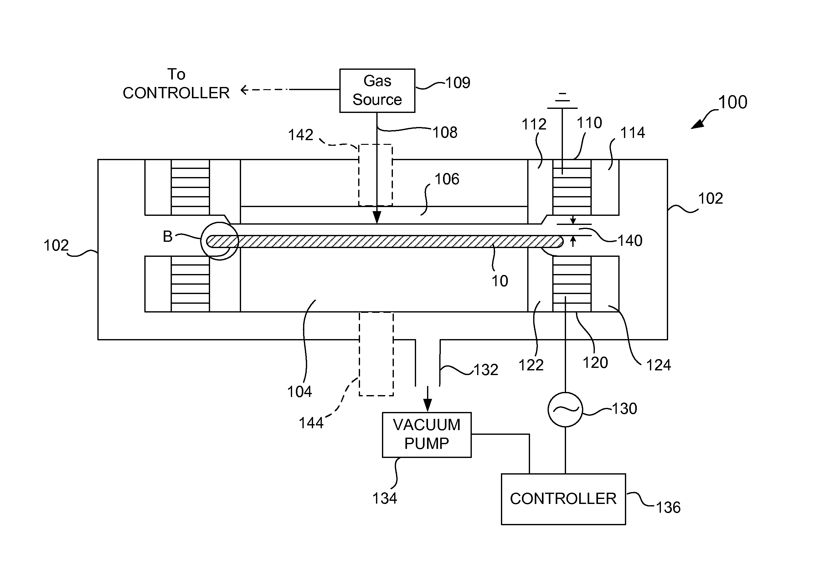
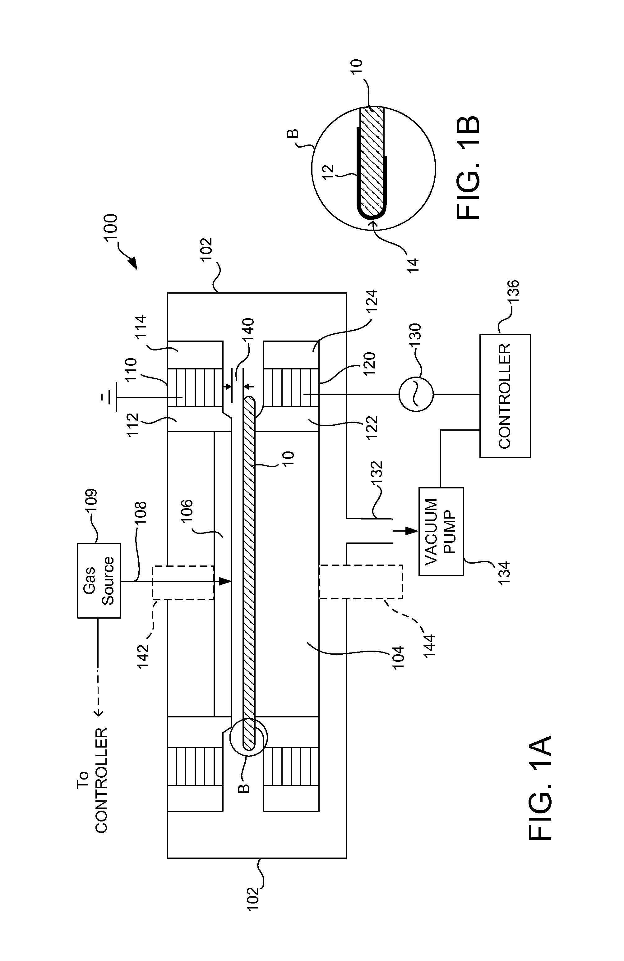
[0037]The present invention will now be described in detail with reference to a few preferred embodiments thereof as illustrated in the accompanying drawings. In the following description, numerous specific details are set forth in order to provide a thorough understanding of the present invention. It will be apparent, however, to one skilled in the art, that the present invention may be practiced without some or all of these specific details. In other instances, well known process steps and / or structures have not been described in detail in order to not unnecessarily obscure the present invention.

[0038]As discussed above, Applicants have identified that the bevel edge of a substrate such as a semiconductor wafer is a primary source of defects due to particle problems and contamination. The bevel edge, in which deposited films terminate and overlap with underlying materials, is exposed to various semiconductor processes such as dry etch or wet clean. The bevel edge of a substrate su...


PUM

PropertyMeasurementUnit
Poweraaaaaaaaaa
Diameteraaaaaaaaaa

Abstract

A method and apparatus for processing a bevel edge is provided. A substrate is placed in a bevel processing chamber and a passivation layer is formed on the substrate only around a bevel region of the substrate using a passivation plasma confined in a peripheral region of the bevel processing chamber. The substrate may undergo a subsequent semiconductor process, during which the bevel edge region of the substrate is protected by the passivation layer. Alternatively, the passivation layer may be patterned using a patterning plasma formed in an outer peripheral region of the processing chamber, the patterning plasma being confined by increasing plasma confinement. The passivation layer on outer edge portion of the bevel region is removed, while the passivation layer on an inner portion of the bevel region is maintained. The bevel edge of the substrate may be cleaned using the patterned passivation layer as a protective mask.

Description

FIELD OF INVENTION[0001]The present invention relates to the formation of semiconductor devices. More particularly, the present invention relates to a method and apparatus for processing a bevel edge of a substrate during the formation of semiconductor devices.BACKGROUND OF THE INVENTION[0002]In the processing of a substrate, e.g., a semiconductor wafer or a glass panel such as one used in flat panel display manufacturing, plasma is often employed. A plurality of dies, or divided rectangular areas, are formed on the substrate, each of which will become an integrated circuit. The substrate is processed in a series of steps in which materials are deposited and selectively removed. Typically, such a substrate is coated with a thin film of hardened emulsion (such as a photoresist mask) prior to etching. Areas of the hardened emulsion are then selectively removed, causing parts of the underlying layer to become exposed. The substrate is then placed on a substrate support structure in a p...

Claims


Application Information

Patent Timeline
IPC IPC(8): B08B5/00C25F1/00
CPCC23C16/0245C23C16/04C23C16/509H01L21/31144H01L21/02115H01L21/02274H01L21/3083H01L21/02087H01L21/02H01L21/02266H01L21/0228H01L21/02631H01L21/0273H01L21/205H01L21/28247H01L21/302H01L21/30621H01L21/3065H01L21/31116H01L21/76825H01L21/76826
Inventor CHEN, JACKKIM, YUNSANG
Owner LAM RES CORP
Why Eureka
Try Eureka