Methods to pattern diffusion layers in solar cells and solar cells made by such methods

a technology of solar cells and diffusion layers, applied in the field of methods to make pattern diffusion layers in solar cells and solar cells by such methods, can solve the problems of reducing the concentration of p and a deep emitter, and reducing the electronic quality of materials, so as to prevent or minimize the reflection of light energy and less precision

Inactive Publication Date: 2011-06-23
1366 TECH INC
View PDF2 Cites 14 Cited by
  • Summary
  • Abstract
  • Description
  • Claims
  • Application Information

AI Technical Summary

Benefits of technology

Methods of exploiting a Self Aligned Cell (SAC) architecture for doping purposes use either the architecture to direct the deposition and application of a material that dopes the substrate, or a material that blocks or retards the substrate from being doped. Some innovations provide doping in the regions that will become metallization for current conducting fingers. The dopant may be treated directly into grooves that have been provided for the purpose. Or, a diffusion-retarding material may be provided in non-groove locations, and dopant may be provided with less precision over the entire surface of the wafer, thereby resulting in only the diffusion-retarder free regions getting the full dopant dose. The SAC architecture also includes grooved or pitted surfaces for the light absorbing regions of a cell, to prevent or minimize reflection away of light energy. The light trapping regions may also be treated with dopant in the grooves, to result in semi-conductor emitter lines within the grooves. Alternatively, a diffusion-retarding material may be treated into the grooves, leaving the upper tips of the ridges between the grooves exposed, thereby subject to deeper, or more significant doping in a subsequent step Similarly, with light trapping pits, a diffusion-retarding material may be treated into the pits, leaving the upper rim of the edges between the pits exposed, thereby subject to deeper doping.

Problems solved by technology

However, a high concentration of P and a deep emitter have drawbacks as well.
The short wavelength light tends to be absorbed very strongly in a thin layer near the top of the wafer in this diffused region, and high P doping levels reduce the electronic quality of the material such that charge carriers more easily recombine at defects before they are able to be collected.
With higher surface P concentrations, it becomes more challenging to obtain good surface passivation with front surface dielectric layers.
Only a very small percentage of present Si solar cell manufacturers employ selective emitters, since the additional processing steps and process complexity needed to create the patterned diffusion are difficult obstacles.
Common methods to produce selective emitters involve at least two high temperature diffusion steps and a difficult alignment of a screen printed metal layer to the heavily diffused pattern.
Known methods of providing a selective emitter have drawbacks.
Another drawback of known selective emitter processing methods is that at least two high temperature treatment steps, each with its attendant preparations, cooling down periods, etc.
Such techniques have drawbacks.
In general, the low thickness or low concentration dopant sources constitute relatively limited availability of dopant for doping, as opposed to a relatively unlimited availability of dopant provided by the dopant dispensed into the grooves or by the glass formed by a long and / or high-flow POCl3 exposure.
Such doping may not be ideal, perhaps by doping more than desired or by being nonuniform across the wafer surface.
For example, if one were to provide a wafer with grooves that are smaller than approximately 50 microns in width, the minimum line widths and the achievable alignment of known ink deposition techniques such as screen printing, pad printing, inkjet printing, direct write nozzle dispensing, etc., are not sufficient to place ink in the groove without ink also being deposited outside the groove regions in an undesirable manner.

Method used


Image

  • Methods to pattern diffusion layers in solar cells and solar cells made by such methods
  • Methods to pattern diffusion layers in solar cells and solar cells made by such methods
  • Methods to pattern diffusion layers in solar cells and solar cells made by such methods

Examples


Embodiment Construction

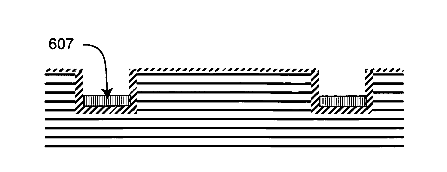
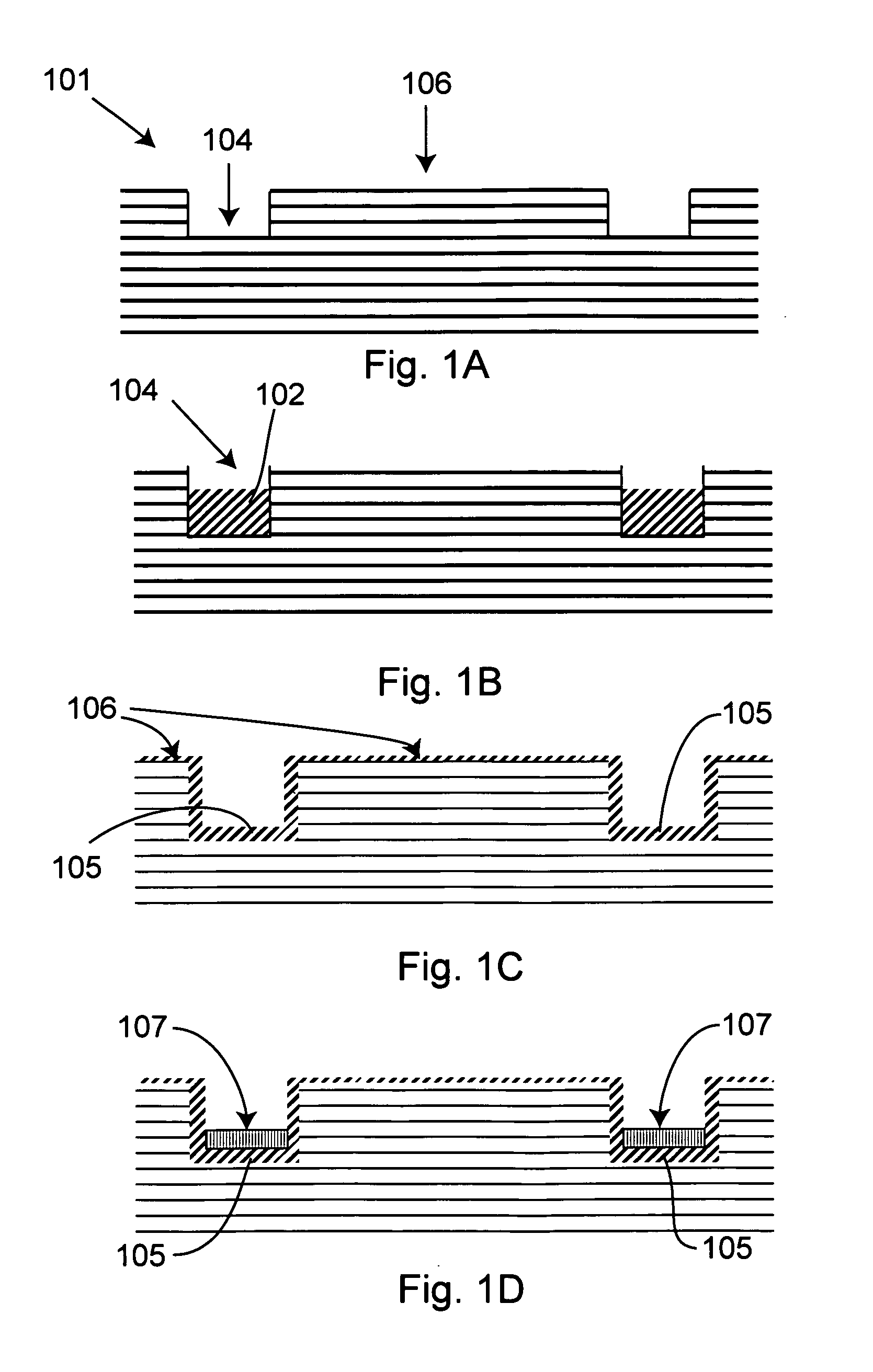
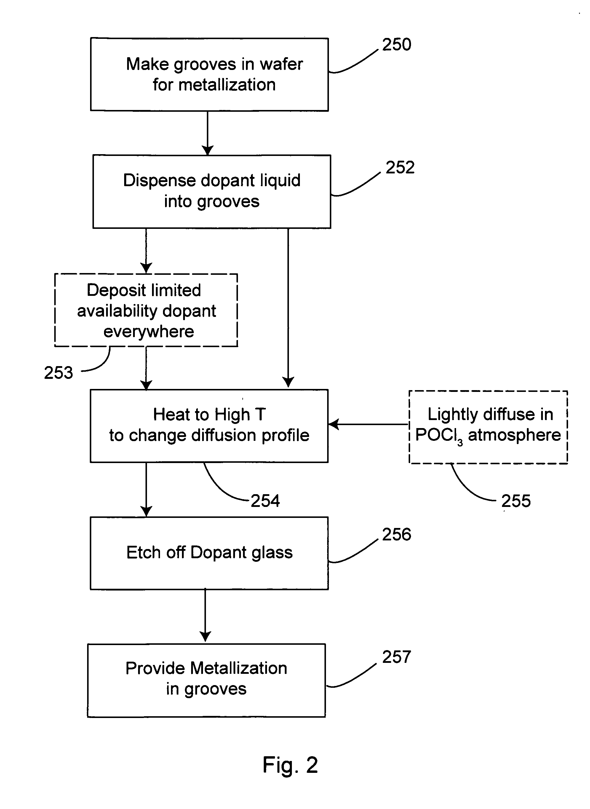
Innovations disclosed herein include but are not limited to ways to form: 1) a selective emitter with deeper diffusion under the metallization areas for good contact resistance and good blue response; and 2) deep emitter gridlines. In contrast to known techniques for providing a selective emitter, which require alignment of a metal layer to the heavily diffused pattern, as well as at least two high temperature steps, the elegance of the general SAC architecture lends itself to implementation of a selective emitter with minimal extra processing and complexity. It is not necessary to maintain two different instances of the same pattern in register, and only one high temperature step is required. The process is self-aligning.

Similarly, it may be more cost effective to use the SAC architecture than to use other processing schemes to provide deep emitter gridlines, for instance perpendicular to conventional metal fingers (oriented in the same manner as the so-called semiconductor fingers...


PUM

PropertyMeasurementUnit
depthaaaaaaaaaa
depthaaaaaaaaaa
groove widthaaaaaaaaaa

Abstract

Methods exploiting a Self Aligned Cell (SAC) architecture for doping purposes, use the architecture to direct the deposition and application of either a dopant or a diffusion retarder. Doping is provided in regions that will become metallization for conducting fingers. Dopant may be treated directly into metallization grooves. Or, diffusion retarder may be provided in non-groove locations, and dopant may be provided over some or all of the entire wafer surface. Dopant and metal automatically go where desired, and in register with each other. The SAC architecture also includes concave surfaces for light absorbing regions of a cell, to reduce reflection of light energy, which regions may also be treated with dopant in the concavities, to result in semiconductor emitter lines. Alternatively, diffusion retarder may be treated into the concavities, leaving upper tips of ridges between the concavities exposed, thereby subject to deeper doping.

Description

The present disclosure describes methods to form a selective emitter that are compatible with the SAC technology.Briefly, the SAC concepts involve the formation of grooves and other features into the surface of Si wafers that allow subsequent processing steps involving the dispensing of solutions into the grooves to perform the operations of etching dielectrics, catalyst application, depositing metals, and masking against subsequent processing activities.Certain processing schemes for providing liquid containing material to a surface are discussed in U.S. Provisional Application 61 / 204,382 entitled, DISPENSING LIQUID CONTAINING MATERIAL TO PATTERNED SURFACES USING A CAPILLARY DISPENSING TUBE, filed on Jan. 6, 2009. This application is incorporated fully herein by reference. The technology disclosed in this application is referred to herein as Capillary Dispensing Technology. The Capillary Dispensing Technology and the provisional application that describes it is explicitly declared ...

Claims


Application Information

Patent Timeline
Patent Type & Authority Applications(United States)
IPC IPC(8): H01L31/0224H01L31/18
CPCH01L21/228H01L21/6715H01L31/022425Y02E10/547H01L31/03529H01L31/1804H01L31/0288Y02P70/50
Inventor GABOR, ANDREW M.WALLACE, RICHARD L.
Owner 1366 TECH INC
Why Eureka
Try Eureka