Semiconductor device

a technology of semiconductors and semiconductors, applied in the direction of capacitors, solid-state devices, instruments, etc., can solve the problems of increased cost per storage capacity, loss of stored data in srams, and difficulty in sufficiently reducing power consumption, so as to achieve the effect of reducing power consumption, ensuring data retention, and ensuring data retention

Inactive Publication Date: 2011-06-30
SEMICON ENERGY LAB CO LTD
View PDF99 Cites 82 Cited by
  • Summary
  • Abstract
  • Description
  • Claims
  • Application Information

AI Technical Summary

Benefits of technology

[0011]In the disclosed invention, a semiconductor device is formed using a purified oxide semiconductor. The transistor formed using a purified oxide semiconductor has an extremely small leakage current, so that data can be stored for a long time.
[0025]Since the off-state current of a transistor including an oxide semiconductor is extremely small, stored data can be retained for an extremely long time by using the transistor. In other words, power consumption can be adequately reduced because refresh operation becomes unnecessary or the frequency of refresh operation can be extremely low. Moreover, stored data can be retained for a long time even when power is not supplied.
[0026]Further, in a semiconductor device according to the disclosed invention, high voltage is not needed to write data, and deterioration of the element does not become a problem. For example, unlike a conventional non-volatile memory, it is not necessary to inject and extract electrons into and from a floating gate, so that a problem such as deterioration of a gate insulating layer does not occur at all. That is, the semiconductor device according to the disclosed invention has no limitation on the number of times of rewriting, which is a problem of a conventional non-volatile memory, and reliability thereof is drastically improved. Further, writing of data is performed depending on an on state and an off state of the transistor, so that high-speed operation can be easily realized. Additionally, there is an advantage that operation for erasing data is not needed.

Problems solved by technology

For that reason, another writing operation (refresh operation) is necessary at predetermined intervals, and it is difficult to sufficiently reduce power consumption.
Furthermore, since stored data is lost when power supply stops, an additional storage device utilizing a magnetic material or an optical material is needed in order to hold the data for a long time.
However, cost per storage capacity is increased because a circuit such as a flip-flop is used.
Moreover, as in a DRAM, stored data in an SRAM is lost when power supply stops.
However, a gate insulating layer included in a storage element deteriorates by tunneling current generated in writing, so that the memory element stops its function after a predetermined number of writing operations.
However, a complicated peripheral circuit is needed to realize this method.
Even when such a method is employed, the fundamental problem of lifetime is not resolved.
In other words, a flash memory is not suitable for applications in which data is frequently rewritten.
Further, it takes a relatively long time to inject or remove electric charge, and it is not easy to perform writing and erasing at higher speed.

Method used


Image

  • Semiconductor device
  • Semiconductor device
  • Semiconductor device

Examples


embodiment 1

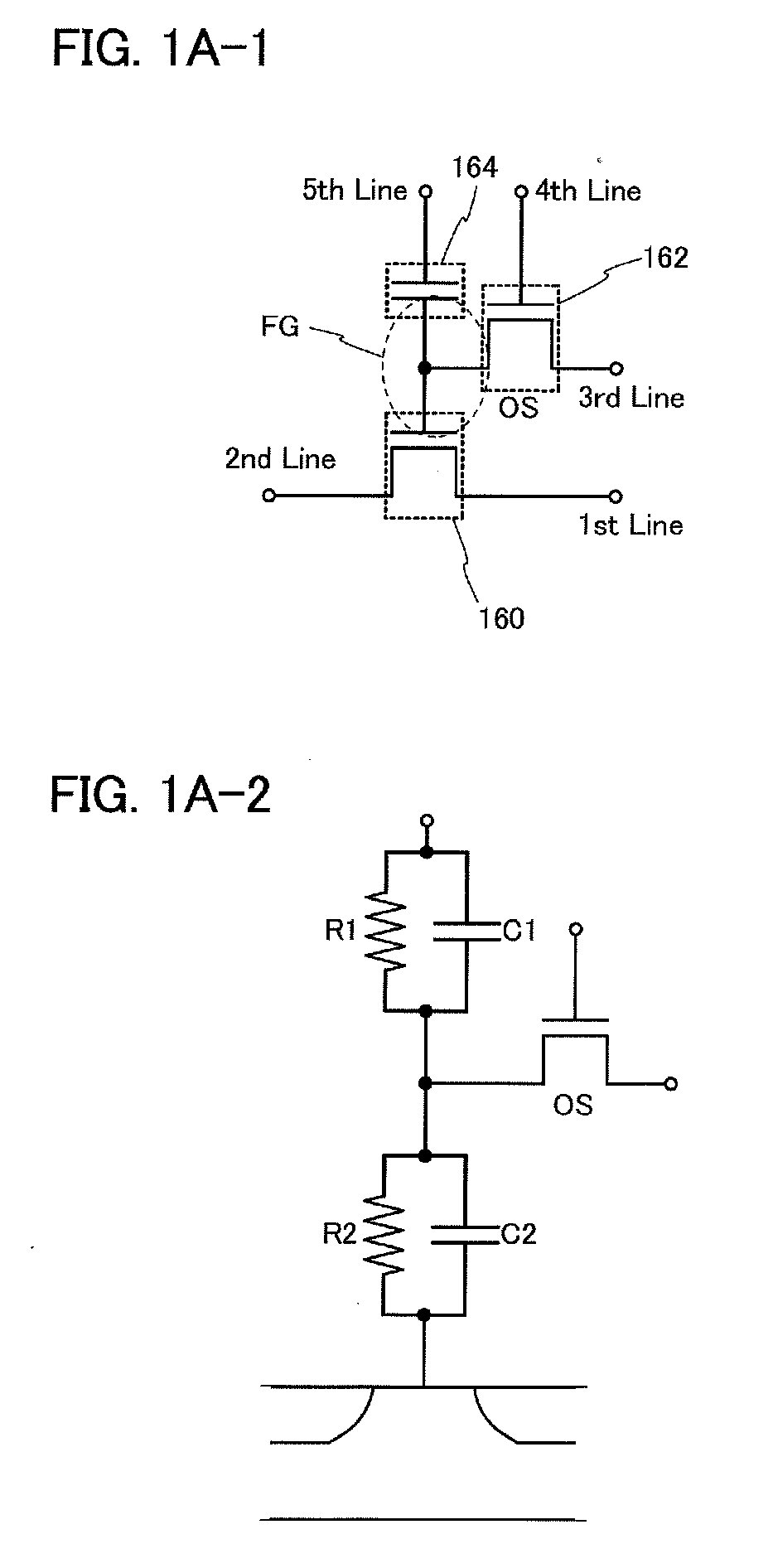
[0059]In this embodiment, a circuit configuration and operation of a semiconductor device according to one embodiment of the disclosed invention will be described with reference to FIGS. 1A-1 and 1A-2. Note that in each of circuit diagrams, “OS” may be written beside a transistor in order to indicate that the transistor includes an oxide semiconductor.

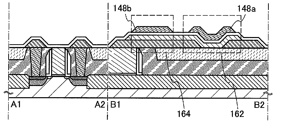
[0060]In the semiconductor device illustrated in FIG. 1A-1, a first wiring (a 1st Line) is electrically connected to a source electrode of a transistor 160, and a second wiring (a 2nd Line) is electrically connected to a drain electrode of the transistor 160. A gate electrode of the transistor 160 and one of a source electrode and a drain electrode of a transistor 162 are electrically connected to one of electrodes of a capacitor 164. A third wiring (a 3rd Line) is electrically connected to the other of the source electrode and the drain electrode of the transistor 162, and a fourth wiring (a 4th Line) is electrically connected to a ga...

embodiment 2

[0096]In this embodiment, an application example of the semiconductor device described in the above embodiment will be described. Specifically, an example of a semiconductor device in which the semiconductor devices described in the above embodiment are arranged in matrix will be described.

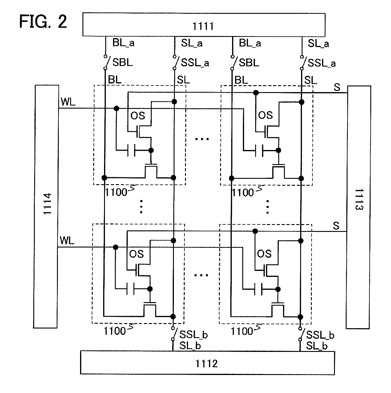
[0097]FIG. 2 is an example of a circuit diagram of a semiconductor device including memory capacity of m×n bits.

[0098]The semiconductor device according to one embodiment of the present invention includes a memory cell array where m word lines WL, m signal lines S, n bit lines BL, n source lines SL and a plurality of memory cells 1100 arranged in matrix of m (rows) (in a vertical direction)×n (columns) (in a horizontal direction) (m and n are natural numbers), and peripheral circuits of a first driver circuit 1111, a second driver circuit 1112, a third driver circuit 1113, and a fourth driver circuit 1114. Here, the structure described in the foregoing embodiment (the structure illustrated in FIG....

embodiment 3

[0125]In this embodiment, another example of a semiconductor device in which the semiconductor devices described in the above embodiments are arranged in matrix will be described.

[0126]FIG. 6 is an example of a circuit diagram of a semiconductor device including memory capacity of m×n bits.

[0127]The semiconductor device according to one embodiment of the present invention includes a memory cell array where m word lines WL, m signal lines S, n bit lines BL, n2 source lines SL, and a plurality of memory cells 1200 arranged in matrix of m (rows) (in a vertical direction)×n (columns) (in a horizontal direction) and peripheral circuits of a first driver circuit 1211, a second driver circuit 1212, a third driver circuit 1213, and a fourth driver circuit 1214 (m, n, and n2 are natural numbers and n2 is the smallest natural number which is greater than or equal to n / 2). Here, the structure described in the foregoing embodiment (the structure illustrated in FIG. 1A-1) is applied to the memor...


PUM


Abstract

The semiconductor device includes a source line, a bit line, a signal line, a word line, memory cells connected in parallel between the source line and the bit line, a first driver circuit electrically connected to the source line and the bit line through switching elements, a second driver circuit electrically connected to the source line through a switching element, a third driver circuit electrically connected to the signal line, and a fourth driver circuit electrically connected to the word line. The memory cell includes a first transistor including a first gate electrode, a first source electrode, and a first drain electrode, a second transistor including a second gate electrode, a second source electrode, and a second drain electrode, and a capacitor. The second transistor includes an oxide semiconductor material.

Description

TECHNICAL FIELD[0001]The invention disclosed herein relates to a semiconductor device employing a semiconductor element and a manufacturing method thereof.BACKGROUND ART[0002]Storage devices employing semiconductor elements are roughly classified into two categories: a volatile storage device that loses stored data when power supply stops, and a non-volatile storage device that retains stored data even when power is not supplied.[0003]A typical example of a volatile storage device is a dynamic random access memory (DRAM). A DRAM stores data in such a manner that a transistor included in a memory element is selected and electric charge is stored in a capacitor.[0004]When data is read from a DRAM, electric charge in a capacitor is lost on the above-described principle; thus, another writing operation is necessary whenever data is read out. Moreover, a transistor included in a memory element has a leakage current (off-state current) between a source and a drain in an off state and elec...

Claims


Application Information

Patent Timeline
Patent Type & Authority Applications(United States)
IPC IPC(8): H01L27/108
CPCG11C16/0425H01L29/7881H01L27/108H01L27/11H01L27/115H01L27/11517H01L27/11551H01L27/1156H01L27/1225H01L28/40H01L27/10805H01L27/11568H01L27/11563H01L29/788H01L27/105H10B12/00H10B10/00H10B41/00H10B69/00H10B41/70H10B41/20H01L29/78645H10B12/30H01L29/7869H01L29/78693H01L29/792H10B12/20H10B43/00H10B43/30
Inventor YAMAZAKI, SHUNPEIKOYAMA, JUNKATO, KIYOSHINAGATSUKA, SHUHEIMATSUZAKI, TAKANORIINOUE, HIROKI
Owner SEMICON ENERGY LAB CO LTD
Why Eureka
Try Eureka