Gold-coated polysilicon reactor system and method

a technology of polysilicon and reactor, which is applied in the direction of silicon compounds, electric/magnetic/electromagnetic heating, crystal growth process, etc., can solve the problems of contaminating the wafer, not suitable for heating and deposition of polysilicon on silicon rods or filaments, etc., to reduce power consumption, reduce emissivity, and reduce the emissivity of the chamber wall

Inactive Publication Date: 2011-06-30
GTAT CORPORATION
View PDF99 Cites 14 Cited by
  • Summary
  • Abstract
  • Description
  • Claims
  • Application Information

AI Technical Summary

Benefits of technology

[0009]The subject invention is directed to a reaction chamber system and related devices and methods for use in the system, in which reduced power consumption can be achieved by providing a thin layer of gold on one or more components inside a reaction chamber. According to the subject invention, a reaction chamber made of stainless steel, alloys, or other materials is coated with a thin layer of gold, preferably at least about 0.1 microns thick, and more preferably about 0.5 to 3.0 microns in thickness. The gold-coated reaction chamber preferably has a lower emissivity, as compared to a conventional stainless steel chamber, thus lowering emissivity of the chamber wall and reducing radiant heat losses. Preferably the reaction chamber is configured for use in a chemical vapor deposition (CVD) process, and in particular, is used for depositing polysilicon in the reaction chamber.
[0010]According to the subject invention, power savings of up to about 30% can be achieved by use of a gold-coated reaction chamber, as compared to conventional uncoated stainless steel reaction chambers. For example, by using a gold coating of at least about 0.1 microns thick, or more preferably about 0.5 to 3.0 microns in thickness inside the chamber, power savings of about 20% to 30% are achievable. Although a gold coating has been found to be suitable if at least about 0.1 microns thick, other thicknesses can be used. In particular, the gold coating should have sufficient thickness to achieve the desired optical properties of low emissivity and high reflectivity. Therefore, if such properties can be obtained with a gold coating thickness below about 0.1 microns, a lower thickness could be utilized in a reaction chamber of the subject invention. Preferably, the gold coating has one or more characteristics such as good adhesion, cohesion, washability, and repairability. The more preferred range of between about 0.5 to 3.0 microns is selected based on a gold coating sufficient to maintain the desired optical properties, and where the surface preferably is substantially uniform.
[0011]While the primary function of the gold coating is to reduce the emissivity and increase the reflectivity of the reaction chamber and reactor internal components so that radiant heat losses are minimized, other advantages and benefits are provided. The systems and methods of the subject invention further can provide decreased heat flux, increased power savings, decreased component operating temperatures, and decreased corrosion of the inner surface of the chamber. As a result of this decreased corrosion, the quality of polysilicon produced can be improved because fewer corrosion products are available to contaminate the polysilicon. In addition, because less power is lost radiantly, less power is necessary to maintain silicon rod temperatures. Moreover, with decreased component temperatures, thermal stresses are reduced and equipment lifetimes can be increased.

Problems solved by technology

However, because silver tarnishes, and thus requires refinishing, it is not preferable to utilize silver inside a reaction chamber, in order to avoid the need for periodic maintenance.
However, the Martin reference specifically discourages the use of gold on internal wall surfaces because of the potential for gold to be transferred to a wafer via vapor phase transfer, which could result in contamination of the wafer.
However, the reaction chamber disclosed in U.S. Pat. No. 4,938,815 is designed for large-scale growth of a wafer that surrounds a heating apparatus configured to be inserted and removed between the reaction chambers, and is not suitable for heating and deposition of polysilicon on silicon rods or filaments.

Method used


Image

  • Gold-coated polysilicon reactor system and method
  • Gold-coated polysilicon reactor system and method
  • Gold-coated polysilicon reactor system and method

Examples


Embodiment Construction

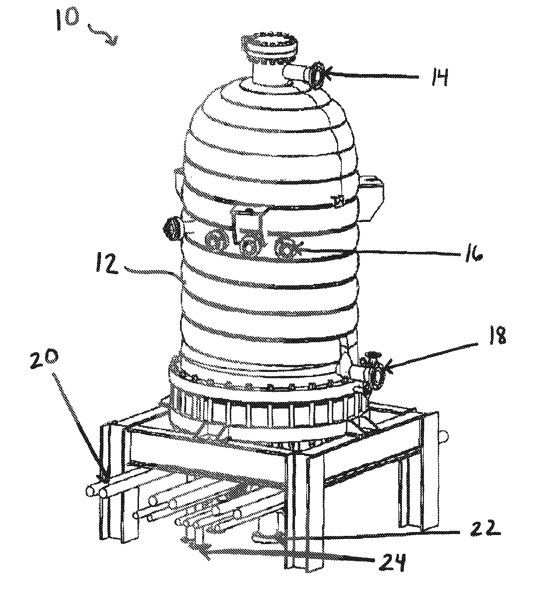
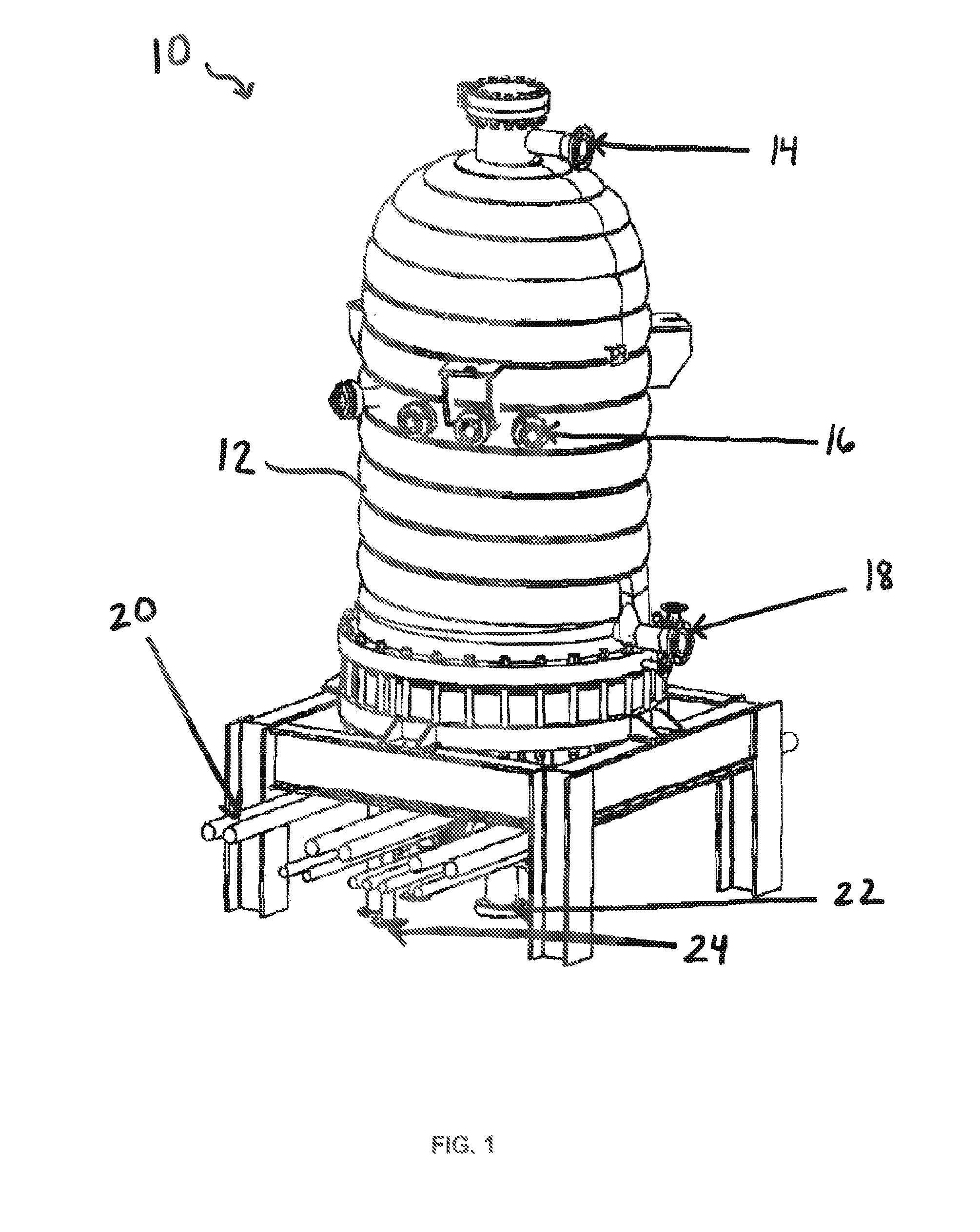
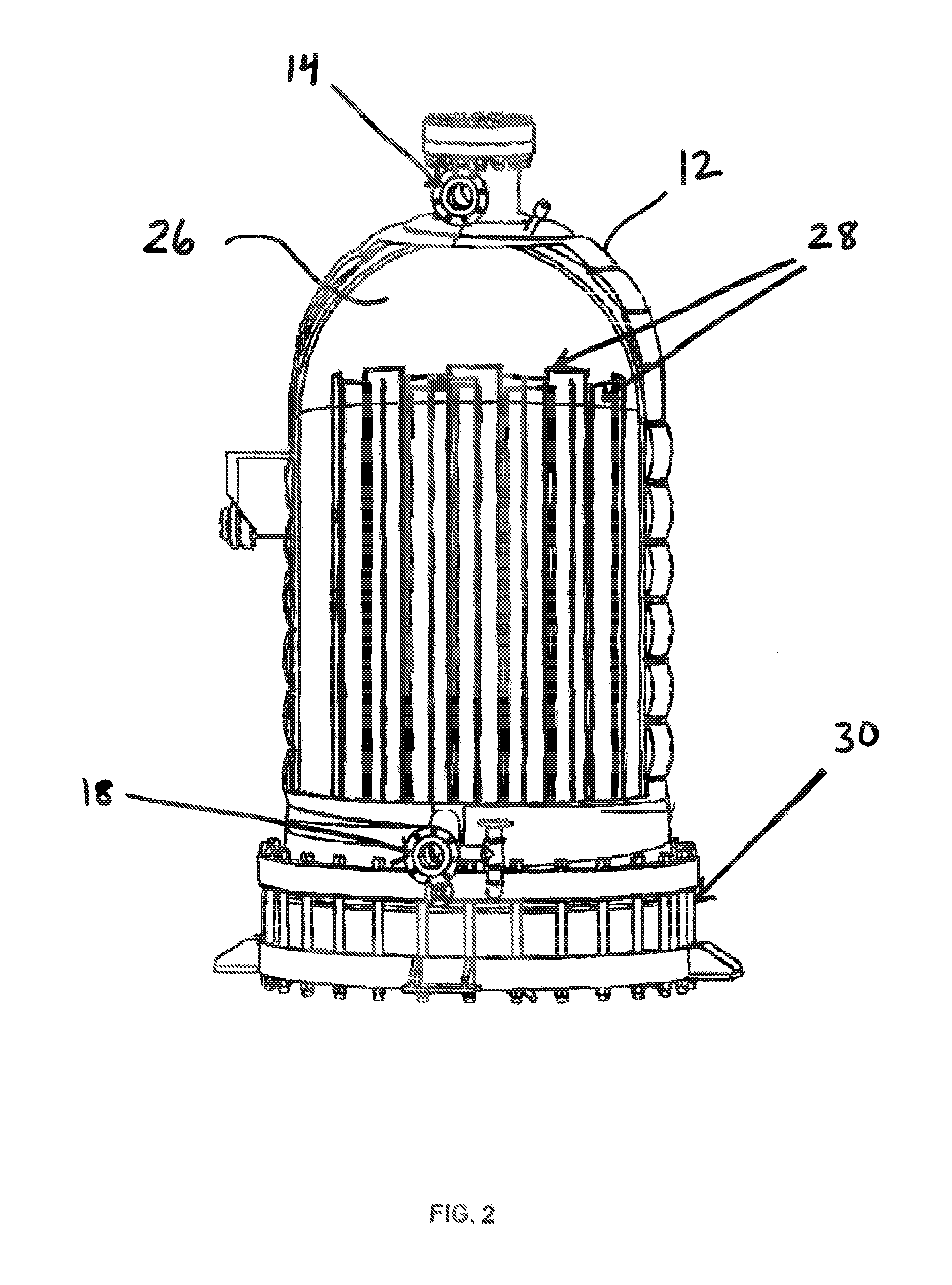
[0018]Preferred embodiments of the subject invention are described below with reference to the accompanying drawings, in which like reference numerals represent the same or similar elements.

[0019]A reaction chamber system, and related devices and methods for use with the system, are provided. The system preferably incorporates a chemical vapor deposition (CVD) reactor, in which polysilicon or another material can be deposited according to the Siemens method. Preferably the system includes a reaction chamber, in which existing power supplies are used. The chamber is used to deposit polysilicon on thin rods or filaments preferably made of silicon, which are heated by passing a current through the thin rods or filaments. The polysilicon deposits accumulate substantially uniformly on exposed surfaces of the filaments within the chamber, substantially without impurities. Alternatively, a material other than polysilicon can be deposited in the reaction chamber.

[0020]During deposition of p...


PUM

PropertyMeasurementUnit
thicknessaaaaaaaaaa
thicknessaaaaaaaaaa
emissivityaaaaaaaaaa

Abstract

A reaction chamber system, and related devices and methods for use in the system, are provided in which reduced power consumption can be achieved by providing a thin layer of gold on one or more components inside a reaction chamber. The reaction chamber system can be used for chemical vapor deposition. The gold coating should be maintained to a thickness of at least about 0.1 microns, and more preferably about 0.5 to 3.0 microns, to provide a suitable emissivity inside the reaction chamber, and thus reduce heat losses.

Description

CROSS-REFERENCE TO RELATED APPLICATION[0001]This application claims priority to U.S. Provisional Application Ser. No. 61 / 039,756, filed on Mar. 26, 2008, the disclosure of which is expressly incorporated herein by reference in its entirety.BACKGROUND OF THE INVENTION[0002]1. Field of the Invention[0003]The subject invention is directed to systems and methods for increasing energy efficiency in chemical vapor deposition reactors. More particularly, the invention relates to systems and methods for reducing power consumption in chemical vapor deposition reaction chamber systems by coating the inside of a reaction chamber with a thin layer of gold to reduce emissivity.[0004]2. Description of the Related Art[0005]In semiconductor fabrication processes and photovoltaic applications utilizing processes such as chemical vapor deposition (CVD), materials can be heated in large furnaces or reaction chambers that require high voltages to achieve melting and / or deposition of various chemical ag...

Claims


Application Information

Patent Timeline
Patent Type & Authority Applications(United States)
IPC IPC(8): C23C16/46C23C16/455C23C16/458C23C16/24
CPCC01B33/035C30B25/08C23C16/4404
Inventor GUM, JEFFREY C.FERO, CHADDESROSIER, DAN
Owner GTAT CORPORATION
Why Eureka
Try Eureka