Three Dimensional Integration With Through Silicon Vias Having Multiple Diameters

a technology of silicon vias and three-dimensional integration, applied in the direction of instruments, photomechanical devices, optics, etc., can solve the problems of adding cost, complexity, process time, etc., to the manufacturing process

Active Publication Date: 2011-07-14
IBM CORP
View PDF53 Cites 64 Cited by
  • Summary
  • Abstract
  • Description
  • Claims
  • Application Information

AI Technical Summary

Benefits of technology

[0006]An alternate exemplary method includes patterning a photoresist layer on a substrate of a structure, the photoresist layer defining an opening having a first area, etching to form a cavity having a first depth in the structure partially defined by the f

Problems solved by technology

The formation of TSVs with complex shapes, such as multiple diameters in a single TSV, has used inefficient fabrication methods u

Method used


Image

  • Three Dimensional Integration With Through Silicon Vias Having Multiple Diameters
  • Three Dimensional Integration With Through Silicon Vias Having Multiple Diameters
  • Three Dimensional Integration With Through Silicon Vias Having Multiple Diameters

Examples


Embodiment Construction

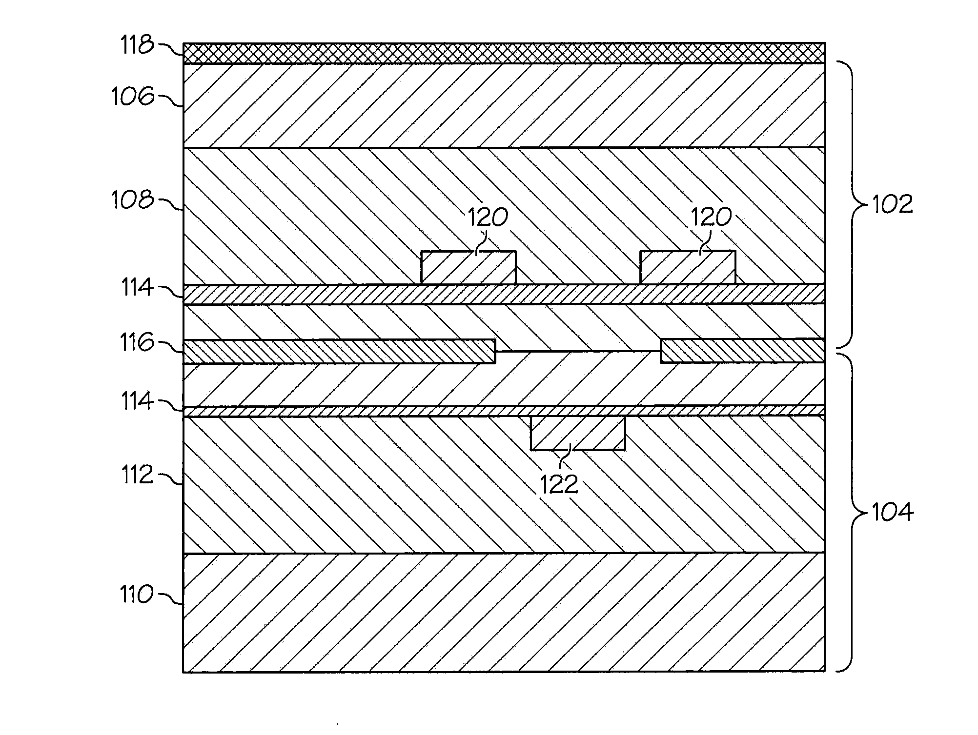
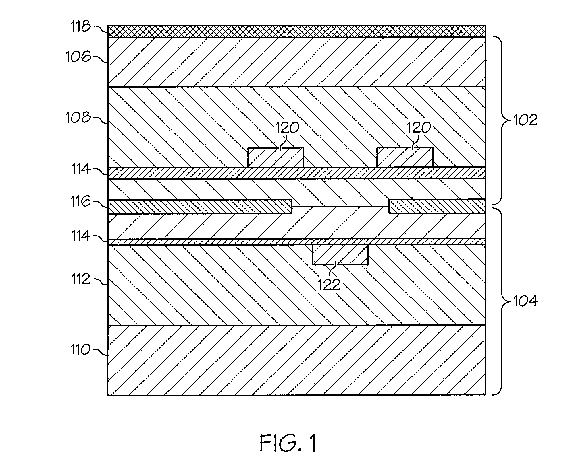
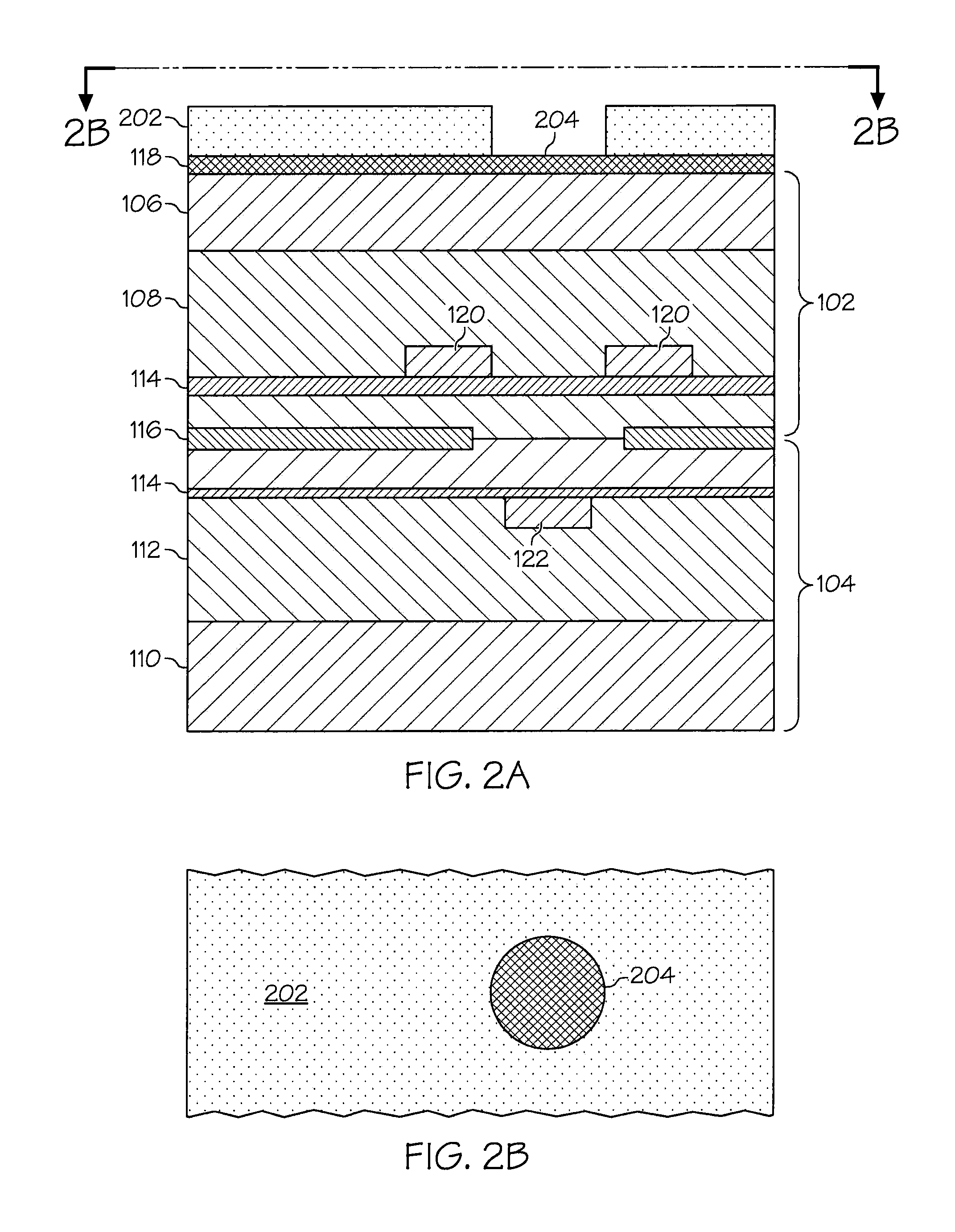
[0012]FIG. 1 illustrates a cross sectional view of an exemplary embodiment of a portion of a three-dimensionally integrated circuit (3D IC) including multiple bonded silicon substrates having a first component 102 arranged on a second component 104. The first component 102 and second component 104 may each be, for example, a silicon wafer or chip, in which the wafer or chip includes front-end-of-line (FEOL), middle-of-line (MOL), and back-end-of-line (BEOL) structures formed thereon, as known in the art. The first component 102 includes a substrate portion 106, which may be a silicon substrate, and a wiring level portion 108, which may comprise a conductive line embedded in a dielectric layer. The substrate portions 106 and 110 consist of a semiconductor material, which may be a single crystalline substrate which may be selected from, but is not limited to, silicon, germanium, silicon-germanium alloy, silicon carbon alloy, silicon-germanium-carbon alloy, gallium arsenide, indium ars...


PUM


Abstract

A method is disclosed which includes patterning a photoresist layer on a substrate of a structure, removing a first portion of the photoresist layer to expose a first area of the substrate, etching the first area to form a cavity having a first depth, removing a second portion of the photoresist to expose an additional area of the substrate, and etching the cavity to expose a first conductor in the structure and the additional area to expose a second conductor in the structure.

Description

BACKGROUND[0001]The present invention relates to semiconductor device manufacturing techniques, specifically fabrication of through silicon vias (TSVs) with multiple diameters.[0002]In the microelectronics industry, packaging density continuously increases in order to accommodate more electronic devices into a package. In this regard, three-dimensional (3D) stacking technology of wafers and / or chips substantially contributes to the device integration process. Typically, a semiconductor wafer includes several layers of integrated circuitry (e.g., processors, programmable devices, memory devices, etc.) built on a silicon substrate. A wafer may be cut into a number of portions to define chips. A top layer of such a chip may be connected to a bottom layer of another such chip by means of through silicon interconnects or vias. In order to form a 3D integrated circuit (IC) stack, two or more chips or wafers are placed on top of one other and bonded.[0003]Previous methods for electrically ...

Claims


Application Information

Patent Timeline
IPC IPC(8): G03F7/20
CPCH01L2225/06565H01L2225/06544H01L21/3085H01L21/76898H01L2924/0002H01L25/0657H01L2924/00
Inventor FAROOQ, MUKTA G.KEI, RAMONAKINSER, EMILY R.LISI, ANTHONY D.WISE, RICHARDYUSUFF, HAKEEM
Owner IBM CORP
Why Eureka
Try Eureka