Heterojunction solar cell with absorber having an integrated doping profile

Inactive Publication Date: 2011-07-21
INST FUR SOLARENERGIEFORSCHUNG
View PDF3 Cites 31 Cited by
  • Summary
  • Abstract
  • Description
  • Claims
  • Application Information

AI Technical Summary

Benefits of technology

[0018]The “field effect” resulting from the doping profile close to the surface nevertheless leads to one kind of charge carrier, that is to say either the holes or the electrons, being kept away from surface defect states such as occur, for example, at the interface between the absorber layer and the heterojunction layer. This effect is also called “field effect passivation” and implies a physical description of the effective surface passivation based on an electrical field. The high doping close to the surface leads in this context to a corresponding band bending which causes a corresponding electrical field close to the surface, which in turn keeps one kind of charge carrier from reaching the surface and the recombination centres present there.
[0019]The inventors of the present invention have found that such a “field effect passivation” can be advantageously used in the formation or production of heterojunction solar cells. As a result of it being possible to keep charge carriers away from the interface between the absorber layer and heterojunction layer due to the field effect, it is possible for lesser requirements to be imposed on the passivating properties of the heterojunction layer or on the quality of the interface. While in conventional heterojunction solar cells, such as are shown, for example, in FIG. 1a, both recombination due to defects at the interface between the absorber layer and the heterojunction layer and recombination within the volume of the heterojunction layer have a considerable influence on the overall properties of the particular heterojunction solar cell, and in particular on its open circuit voltage, these influences are greatly moderated in the heterojunction solar cell proposed here. Due to the field effect caused by the high doping close to the surface, the charge carriers generated within the absorber layer can for the most part no longer diffuse to the surface of the absorber and recombine at the recombination centres present there. The requirement with respect to a very low surface recombination at the interface between the absorber layer and the heterojunction layer, such as is conventionally chiefly to be achieved in

Problems solved by technology

This additional “series resistance” can lead to a reduction in the f

Method used


Image

  • Heterojunction solar cell with absorber having an integrated doping profile
  • Heterojunction solar cell with absorber having an integrated doping profile
  • Heterojunction solar cell with absorber having an integrated doping profile

Examples


Example

[0049]All the figures are merely diagrams and are not true to scale. In the figure, similar or identical elements are labelled with the same reference signs.

DETAILED DESCRIPTION OF PREFERRED EMBODIMENTS

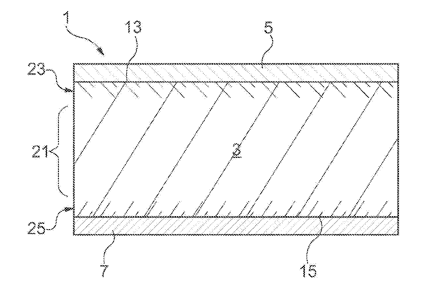
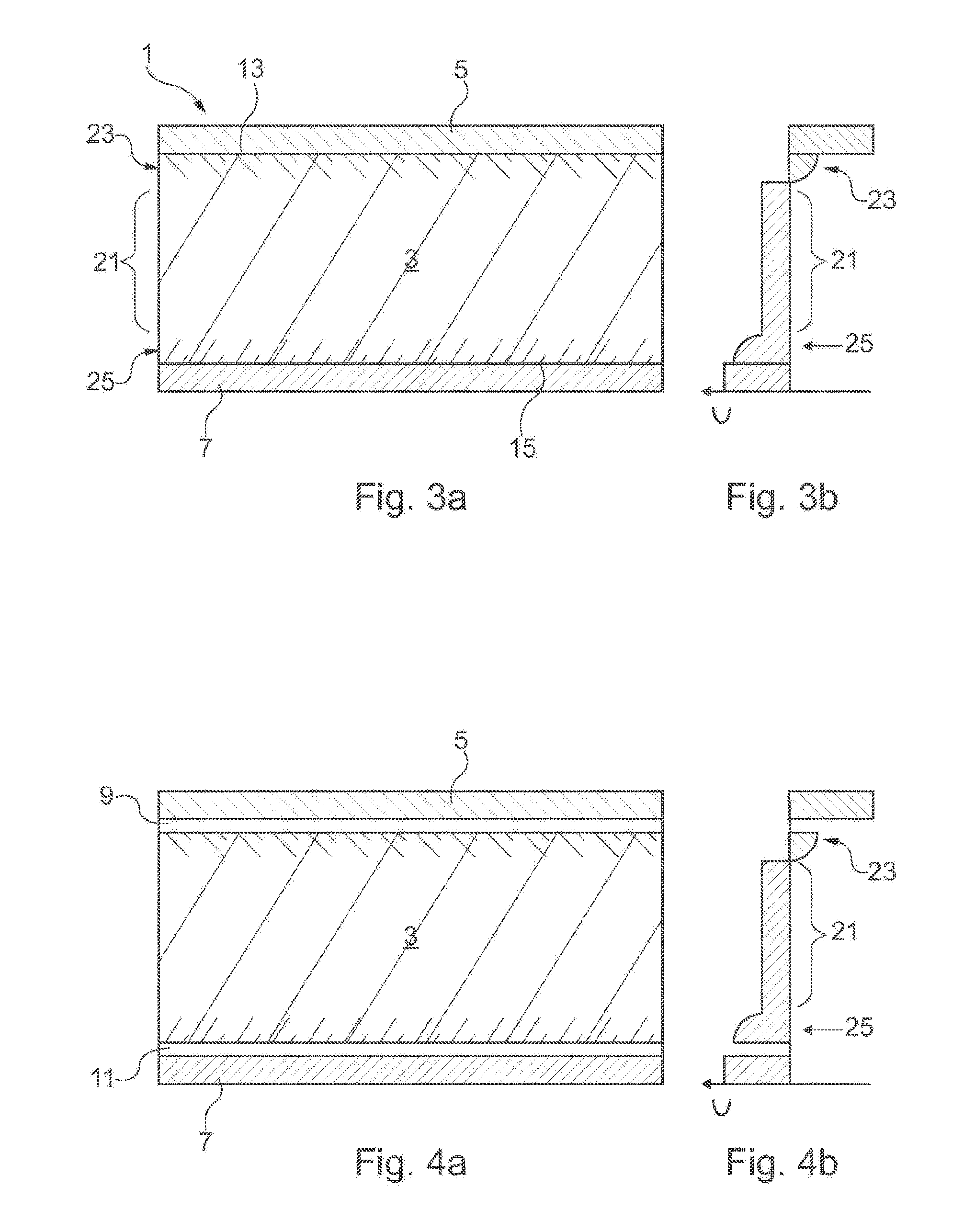
[0050]FIG. 3a shows a heterojunction solar cell 1 according to one embodiment of the present invention. An absorber layer 3 of crystalline silicon is doped, as shown in diagram form in the diffusion profile shown in FIG. 3b, homogeneously in a p-type manner in a central region 21. A doped layer 23, 25 with a doping profile is additionally introduced in regions close to the surface. As can be clearly seen in FIG. 3b and is also shown in diagram form by the nature of the shading in FIG. 3a, the doping agent concentration C in each case decreases in the direction away from the interface 13, 15 of the absorber layer 3 and towards the inside of the absorber layer 3. The nature of the presentation of the doping concentration chosen in FIG. 3b (and 1b, 2b and 4b) is to be understood as meani...


PUM


Abstract

The invention relates to a heterojunction solar cell and a method for the production thereof. The heterojunction solar cell has an absorber layer made of silicon with a basic doping and at least one heterojunction layer of a doped semiconductor material whose band gap differs from that of the silicon of the absorber layer. The absorber layer has a doped layer at an interface directed toward the heterojunction layer, the doping concentration of said doped layer being greater than the basic doping concentration of the absorber layer. As a result of this doping profile, a field effect can be caused which prevents charge carrier pairs produced within the absorber layer from diffusing toward the interface between the absorber layer and the heterojunction layer and from recombining there.

Description

FIELD OF THE INVENTION[0001]The present invention relates to a heterojunction solar cell and a production method for such a heterojunction solar cell.BACKGROUND OF THE INVENTION[0002]Solar cells serve to convert light into electrical energy. In order to be able to spatially separate the charge carrier pairs generated by incident light in a solar cell substrate, the solar cell comprises different adjacent semiconductor regions, the individual regions having electrical properties which differ from each other due to the energy band structure of the semiconductor materials used for the regions and / or due to the nature and concentration of the doping agents introduced into the particular semiconductor material. Due to these different electrical properties, an electrical potential difference is established at the interface between the different semiconductor regions, on the basis of which the electrons and holes of the light-generated charge carrier pairs are spatially separated.[0003]A d...

Claims


Application Information

Patent Timeline
IPC IPC(8): H01L31/0376H01L31/0264H01L31/036H01L31/0352H01L31/0745
CPCH01L31/028H01L31/03762H01L31/0747Y02E10/548Y02E10/547H01L31/0745
Inventor HARDER, NILS-PETER
Owner INST FUR SOLARENERGIEFORSCHUNG
Why Eureka
Try Eureka