Method for manufacturing semiconductor light-emitting device

a technology of semiconductor light-emitting device and manufacturing method, which is applied in the manufacturing of semiconductor/solid-state devices, semiconductor devices, electrical equipment, etc., can solve the problems of difficult discharge of n2 gas, less reliable, and increased heat generated by these light-emitting elements, so as to avoid the cracking of semiconductor films

Active Publication Date: 2011-07-21
STANLEY ELECTRIC CO LTD
View PDF1 Cites 15 Cited by
  • Summary
  • Abstract
  • Description
  • Claims
  • Application Information

AI Technical Summary

Benefits of technology

[0011]According to the method for manufacturing a semiconductor light-emitting device of the present invention, the breakdown of the resin near the semiconductor film in the first laser exposure step forms a space on the perimeter of the semiconductor film. As a result, the N2 gas generated by the semiconductor film in the second laser exposure step can be released via the space. Because N2 gas is not retained on the semiconductor film and high pressure does not occur, cracking o

Problems solved by technology

However, the amount of heat generated by these light-emitting elements has risen along with output, and this heat has made them less reliable.
In such a resin-embedded semiconductor light-emitting device, the following problem occurs when the growth substrate is delaminated using the laser lift-off method.
It is difficult to discharge the N2 gas at this time, and so it collects near the interface betwe

Method used


Image

  • Method for manufacturing semiconductor light-emitting device
  • Method for manufacturing semiconductor light-emitting device
  • Method for manufacturing semiconductor light-emitting device

Examples


1st embodiment

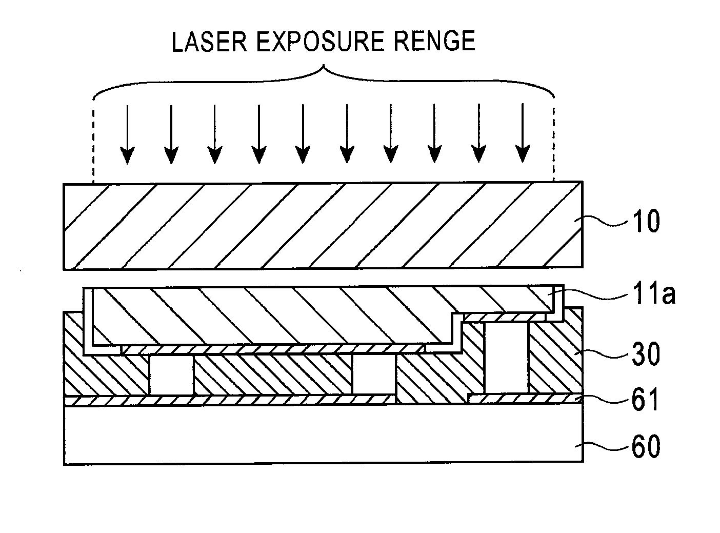
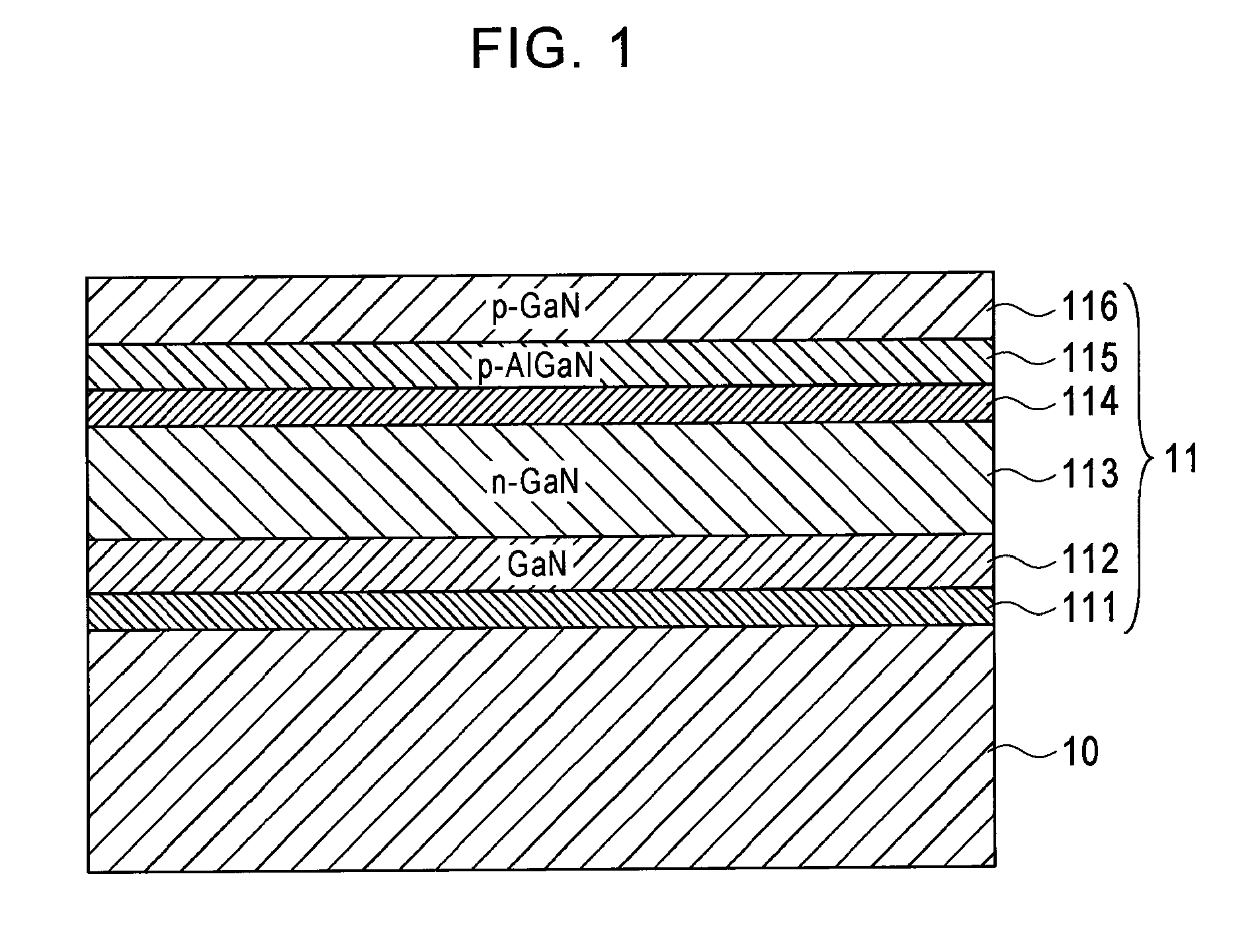
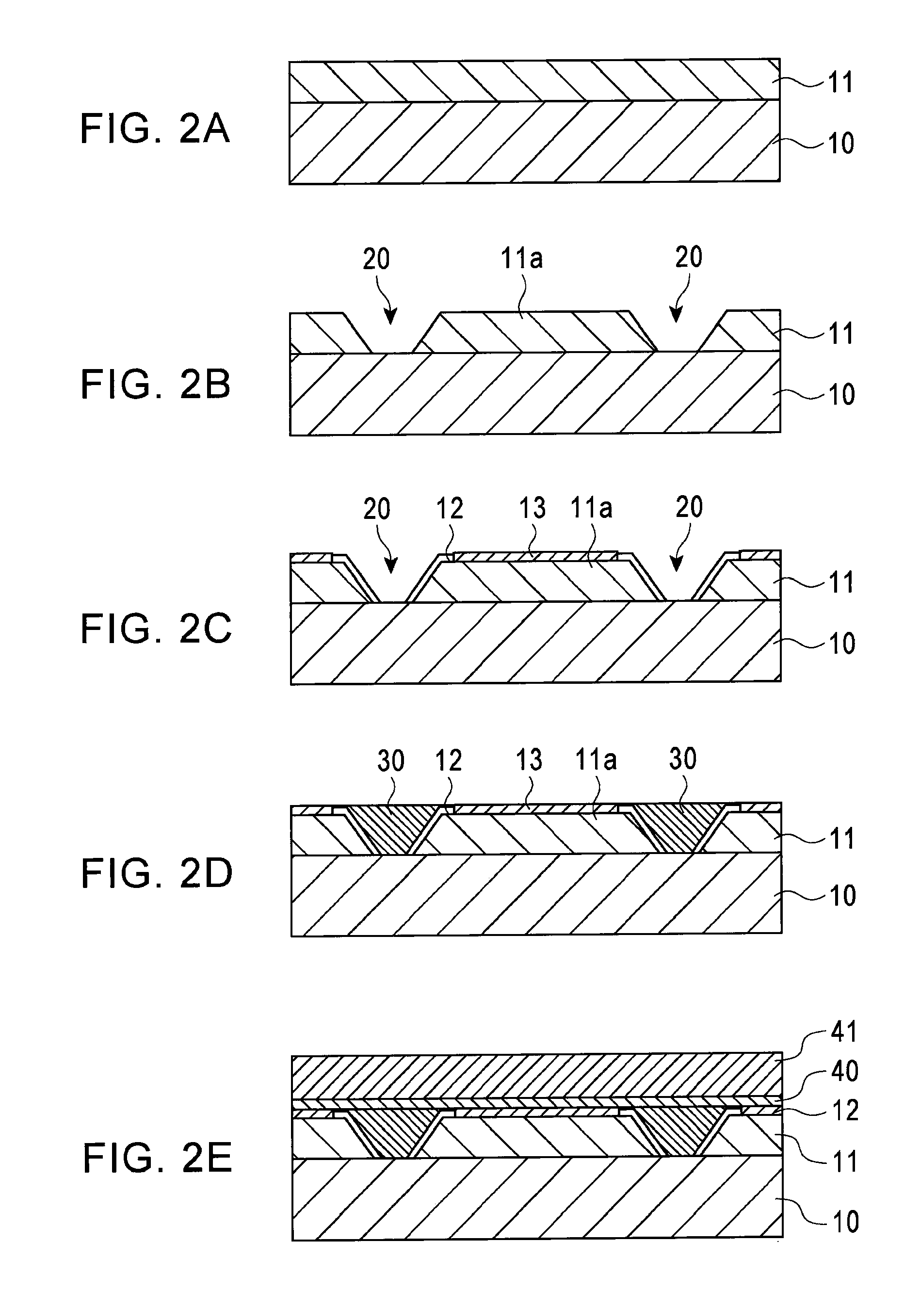
[0023]FIG. 1 is a cross-sectional view representing the layer structure of the semiconductor film 11 according to an embodiment of the present invention. FIGS. 2A through 2E and FIG. 3A through FIG. 3D are cross-sectional views representing the method for manufacturing a semiconductor light-emitting device according to the first embodiment of the present invention. The semiconductor light-emitting device of the first embodiment has a configuration in which the semiconductor film whose crystals were grown epitaxially on top of the growth substrate is supported by Cu film formed using the electroplating method.

(Semiconductor Film Forming Step)

[0024]A sapphire substrate 10 is prepared as the growth substrate for the semiconductor film. The sapphire substrate 10 is heated for ten minutes at 1000° C. in a hydrogen atmosphere, and thermally cleaned. A semiconductor film 11 comprising a low temperature buffer layer 111, an underlying GaN layer 112, an n-GaN layer 113, an active layer 114, ...

2nd embodiment

[0037]FIG. 7A through FIG. 7E and FIG. 8A through FIG. 8E are cross-sectional views showing the method for manufacturing a semiconductor light-emitting device according to the second embodiment of the present invention. In the semiconductor light-emitting device according to the second embodiment, the semiconductor film whose crystals were grown epitaxially on top of a growth substrate are supported by an Si substrate prepared separately.

[0038]An AlxInyGazN semiconductor film 11 is formed on top of a sapphire substrate 10 by performing MOCVD on the surface of the sapphire substrate 10. The structure and growing conditions for the semiconductor film 11 are the same as those in the first embodiment (FIG. 7A). Next, element-dividing grooves 20 demarcating the various semiconductor light-emitting devices are formed in the semiconductor film 11. As in the first embodiment, these element-dividing grooves 20 are formed by performing dry etching using, for example, Cl2 plasma. The semicondu...

3rd embodiment

[0048]FIG. 9A through FIG. 9E and FIG. 10A through FIG. 10B are cross-sectional views showing the method for manufacturing a semiconductor light-emitting device in the third embodiment of the present invention. In the semiconductor light-emitting device of the third embodiment, a semiconductor film 11 whose crystals were grown epitaxially on top of a growth substrate is a flip-chip connected to the top of a submount. The semiconductor film is formed on the surface of a sapphire substrate 10 using MOCVD. The structure and growing conditions of the semiconductor film are the same as those in the first embodiment. Afterwards, the n layer is exposed by etching the semiconductor film via a predetermined resist mask. Next, element-dividing grooves 20 are formed in the semiconductor film to demarcate the individual semiconductor light-emitting devices. The semiconductor film can then be divided into sections 11a which are 1000 μm on a side. Next, the p electrodes 13 and n electrodes 14 are...


PUM


Abstract

A method for manufacturing a resin-embedded semiconductor light-emitting device that is capable of preventing a semiconductor film from being damaged when a growth substrate is delaminated using a laser lift-off method, and that is capable of preventing foreign matter from adhering to the semiconductor film when a resin material is applied. A laser exposure step to delaminate the growth substrate from the semiconductor film comprises a first laser exposure step for performing laser exposure at an energy density at which the resin is broken down but the semiconductor film is not broken down, in a range including a portion adjacent to at least one section of the semiconductor film divided by dividing grooves and at least one section of resin, and a second exposure step for performing laser exposure at an energy density at which the semiconductor film can be broken down in a range including at least one section.

Description

BACKGROUND OF THE INVENTION[0001]1. Field of the Invention[0002]The present invention relates to a semiconductor light-emitting device such as a light-emitting diode (LED), and more particularly to a method for manufacturing a semiconductor light-emitting device including a step in which the growth substrate used for crystal growth of the semiconductor film is removed using a laser lift-off method.[0003]2. Description of the Related Art[0004]Recent advances in technology have increased the efficiency and output of light-emitting elements such as light-emitting diodes (LEDs). However, the amount of heat generated by these light-emitting elements has risen along with output, and this heat has made them less reliable. In order to solve this problem, the growth substrate, which has relatively low thermal conductivity, has been removed, and replaced by a metal with relatively high thermal conductivity to support the semiconductor film. In addition to improving the heat radiating properti...

Claims


Application Information

Patent Timeline
IPC IPC(8): H01L33/48
CPCH01L21/268H01L33/0079H01L33/007H01L33/0093
Inventor IWAYAMA, SHOAKAGI, TAKANOBU
Owner STANLEY ELECTRIC CO LTD
Why Eureka
Try Eureka