Leakage aware design post-processing

a post-processing and leakage detection technology, applied in the direction of originals for photomechanical treatment, instruments, optics, etc., can solve the problems of ed-opc more time-consuming and costly than conventional opc, and the inability to print perfect polygons, etc., to achieve cost-effective effects

Inactive Publication Date: 2011-07-21
GLOBALFOUNDRIES INC
View PDF6 Cites 5 Cited by
  • Summary
  • Abstract
  • Description
  • Claims
  • Application Information

AI Technical Summary

Benefits of technology

[0009]The present invention provides a method, computer program product and computer system for designing a lithographic mask in which the on-wafer target shape is modified to optimize or improve an electrical characteristic, within a predetermined electrical criterion,

Problems solved by technology

However, under low-k1 lithography processes typically in use, the printing of perfect polygons is practically impossible to achieve.
This in turn leads to errors in electrical properties of the printed patterns relative to the desired design.
However, ED-OPC is more time consuming and costly than conventional OPC.
However, the method disclosed by Culp et al. is implemented during the design phase and is not easily modified to account for process variations which may not be known during the design phase.

Method used


Image

  • Leakage aware design post-processing
  • Leakage aware design post-processing
  • Leakage aware design post-processing

Examples


Embodiment Construction

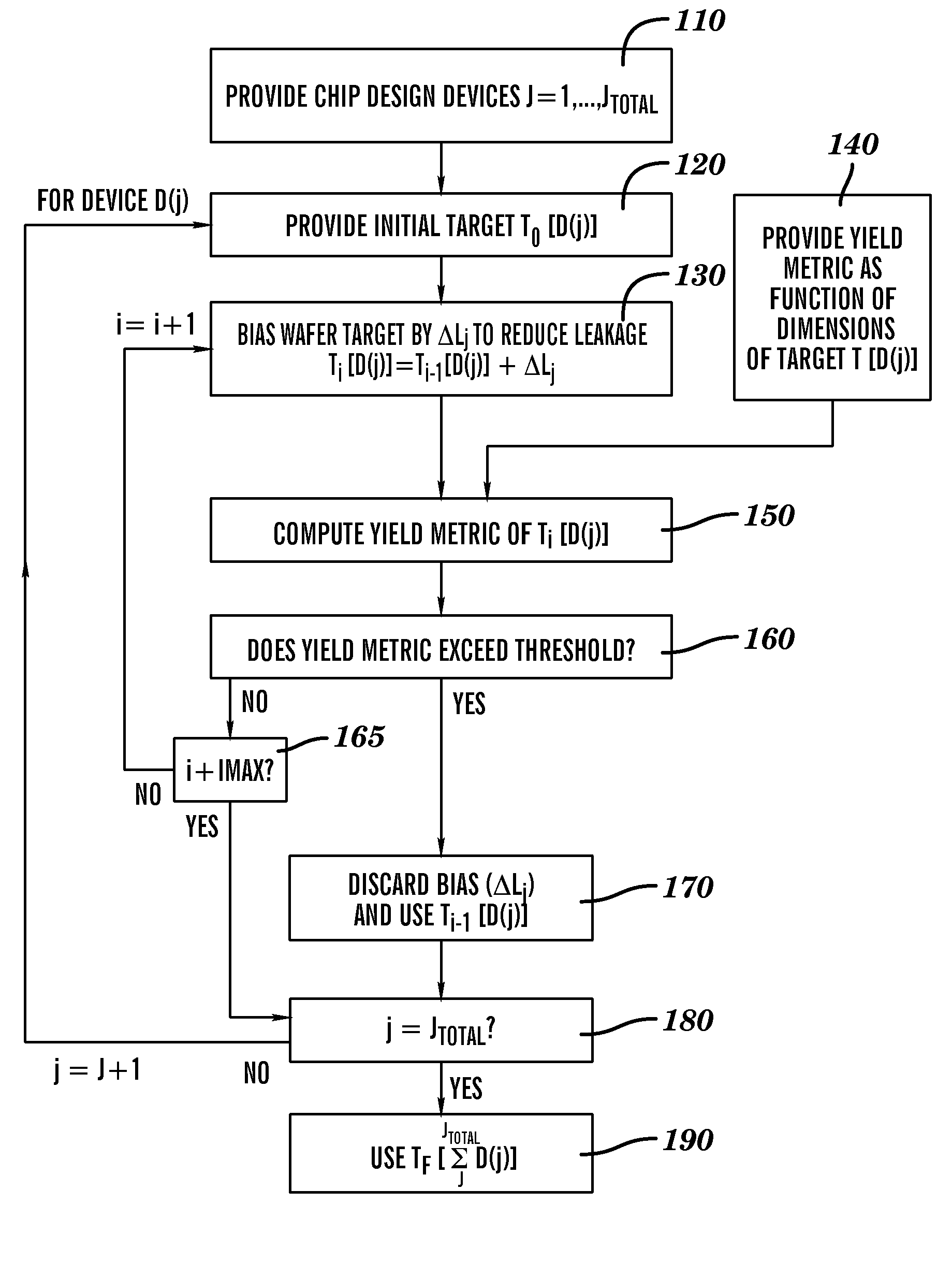
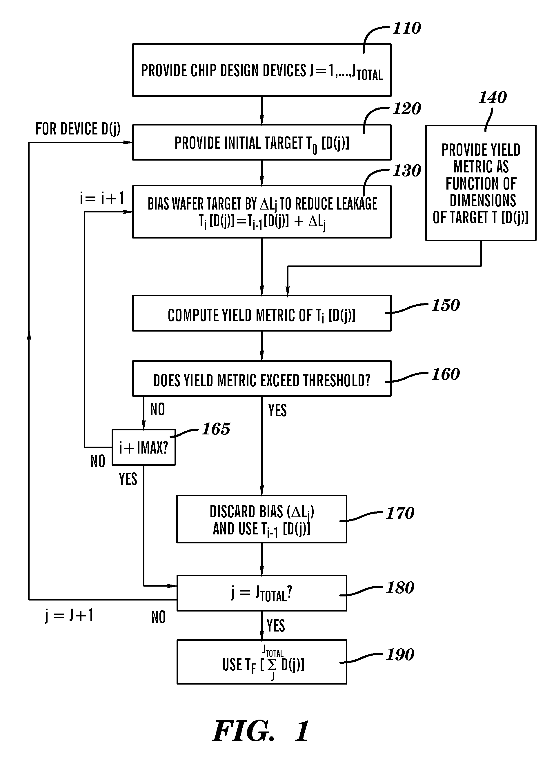
[0025]This invention presents a method for designing and optimizing a lithographic mask that accounts for lithographic process variations across the layout while meeting designers' intent for product requirements. The term “lithographic process” as used and referred to herein, includes, without limitation, any pattern transfer process, such as forming a resist image, forming implants, performing a patterned etch, etc. An integrated circuit design or chip design typically includes layouts of multiple layers of shapes to be printed. A device layer may be printed by using one or more lithographic masks. The on-wafer target is used by an OPC tool or OPC verification tool during the mask design process by ensuring or verifying that simulated image contours resulting from the mask (or masks) for printing a given layer matches the on-wafer target according to predetermined criteria. More particularly, the method, in accordance with the invention, modifies the initial design target by optim...


PUM


Abstract

The present invention provides a method and computer program product for designing an on-wafer target for use by a model-based design tool such as OPC or OPC verification. The on-wafer target is modified by modifying a critical dimension so as to improve or optimize an electrical characteristic, while also ensuring that one or more yield constraints are satisfied. The use of an electrically optimized target can result in cost-effective mask designs that better meet the designers' intent.

Description

FIELD OF THE INVENTION[0001]The present invention broadly relates to the design of integrated circuits, particularly to the design of lithographic masks, and more particularly to improvements in creating targets for use in model-based optical proximity correction (MBOPC) or OPC Verification tools used in mask design processes.BACKGROUND[0002]In the manufacture of integrated circuits, photolithographic processes are commonly used, in which a wafer is patterned by projecting radiation through a patterned mask to form an image pattern on a photo sensitive material, referred to as a photoresist, or simply resist. The exposed resist material is developed to form openings corresponding to the image pattern, and then the pattern is transferred to the wafer substrate by methods such as etching, as known in the art.[0003]The basic lithography system consists of a light source, a photomask containing the pattern to be transferred to the wafer, a collection of lenses, and a means for aligning ...

Claims


Application Information

Patent Timeline
IPC IPC(8): G06F17/50
CPCG06F17/5081G03F1/36G06F30/398
Inventor CULP, JAMES A.LIEBMANN, LARS W.
Owner GLOBALFOUNDRIES INC
Why Eureka
Try Eureka