Nanocarbon material-composite substrate and manufacturing method thereof

a technology of nano-carbon materials and composite substrates, which is applied in the direction of luminescent compositions, transportation and packaging, coatings, etc., can solve the problems of difficult control of the particle diameter or chemical state of metals to be used as catalysts, low carbon nanotube yield, and difficult to achieve uniform thickness and configuration of carbon nanotubes to be created, etc., to achieve easy formation of nano-carbon materials, high aspect ratio, and large surface area

Inactive Publication Date: 2011-07-28
TOPPAN PRINTING CO LTD
View PDF8 Cites 17 Cited by
  • Summary
  • Abstract
  • Description
  • Claims
  • Application Information

AI Technical Summary

Benefits of technology

[0023]According to the nanocarbon material-composite substrate of the present invention, since the nanocarbon material can exist at least on the sidewall portion of a three-dimensional structural pattern, it is possible to utilize a large surface area and a high aspect ratio both originating from the three-dimensional structural pattern.
[0024]According to the method of manufacturing a nanocarbon material-composite substrate of the present invention, it is possible to easily form a nanocarbon material on the sidewall portion of a three-dimensional structural pattern at a low cost while uniformly controlling the configuration of the nanocarbon material.

Problems solved by technology

Among these methods, since the arc discharging method, the laser abrasion method and the plasma chemical vapor deposition method are executed through the utilization of a non-equilibrium reaction, various problems occur, as is generally known.
Namely, amorphous components are more likely to be produced, the carbon nanotube yield is low, and the thickness and kinds (configuration) of carbon nanotube to be created are non-uniform.
This method however is accompanied with problems that it is difficult to control the particle diameter or chemical state of metals to be employed as a catalyst and that it is impossible to synthesize a nanocarbon material which is controlled in configuration and in thickness.
Namely, it is impossible to optionally obtain a nanocarbon material having a desired structure demanded in a specific actual use, resulting in that it is impossible to avoid deterioration of yield.
For these reasons, it has been impossible to manufacture desired parts such as electrodes, etc., at low costs by making use of a large quantity of a nanocarbon material having a desired configuration.
Even if the nanocarbon material of this kind is turned into a paste or mixed with other kinds of material such as a resin, etc., in order to make it useful as a practical material, it has been difficult to obtain a uniform mixture because of the fact that the aggregate of the nanocarbon materials is a disordered mass having a low density.
However, when the aspect ratio of a substrate is increased, it is difficult to enable a raw material to reach a deep inner portion of the substrate.
As a result, it has been difficult to deposit a uniform nanocarbon material in a structure exhibiting a large aspect ratio.
Therefore, no one has succeeded as yet to obtain such a structure that is suited for use in the above-described end-uses, that is formed of highly densified nanocarbon material, and that makes it possible to utilize a large surface area and a high aspect ratio.
Although it is possible to create a carbon nanotube film on the surface of cathodes by making use of the aforementioned method, it is difficult to orientate the carbon nanotube film relative to the surface of the substrate.

Method used


Image

  • Nanocarbon material-composite substrate and manufacturing method thereof
  • Nanocarbon material-composite substrate and manufacturing method thereof
  • Nanocarbon material-composite substrate and manufacturing method thereof

Examples


example

[0066]Followings are explanation of specific examples of the present invention.

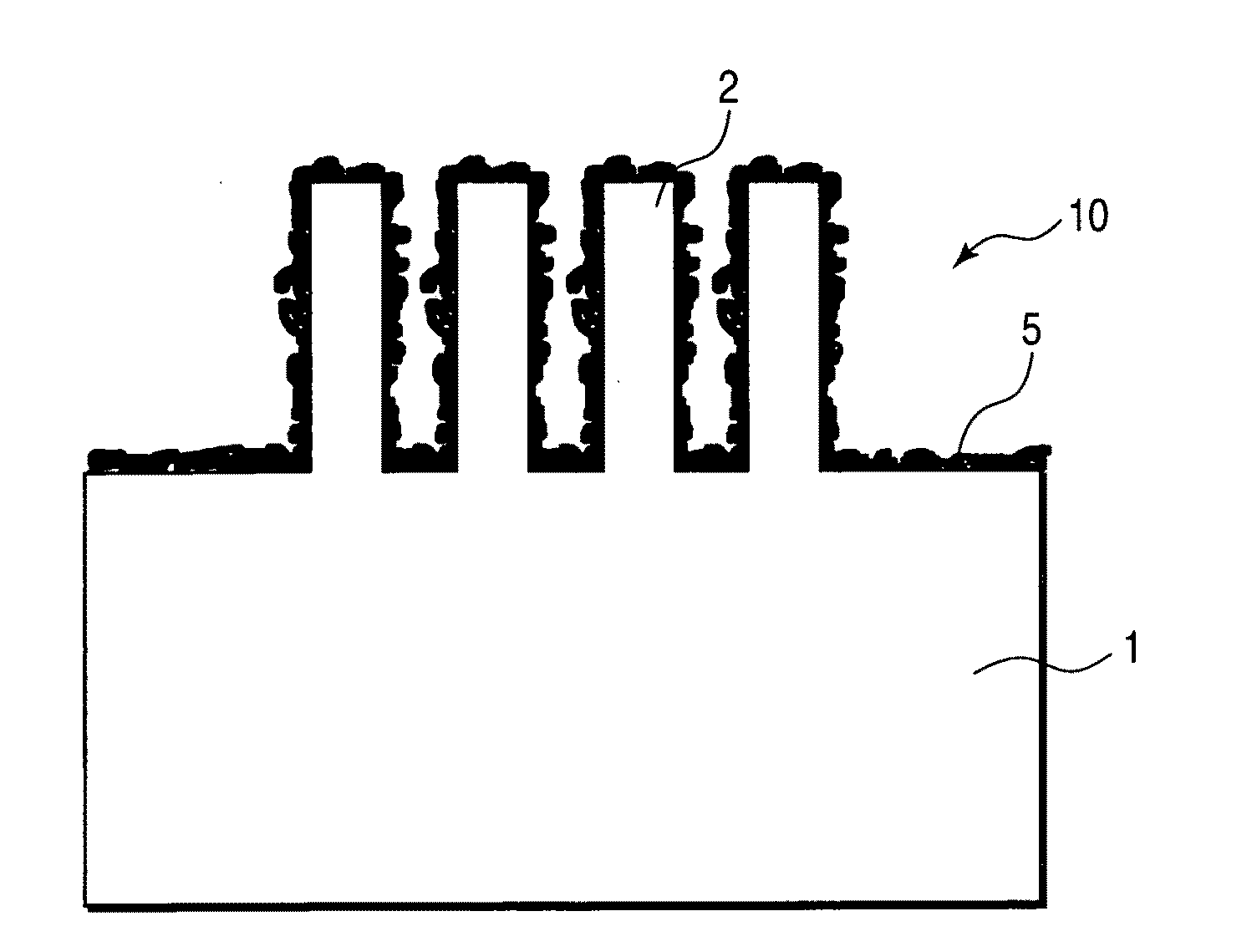
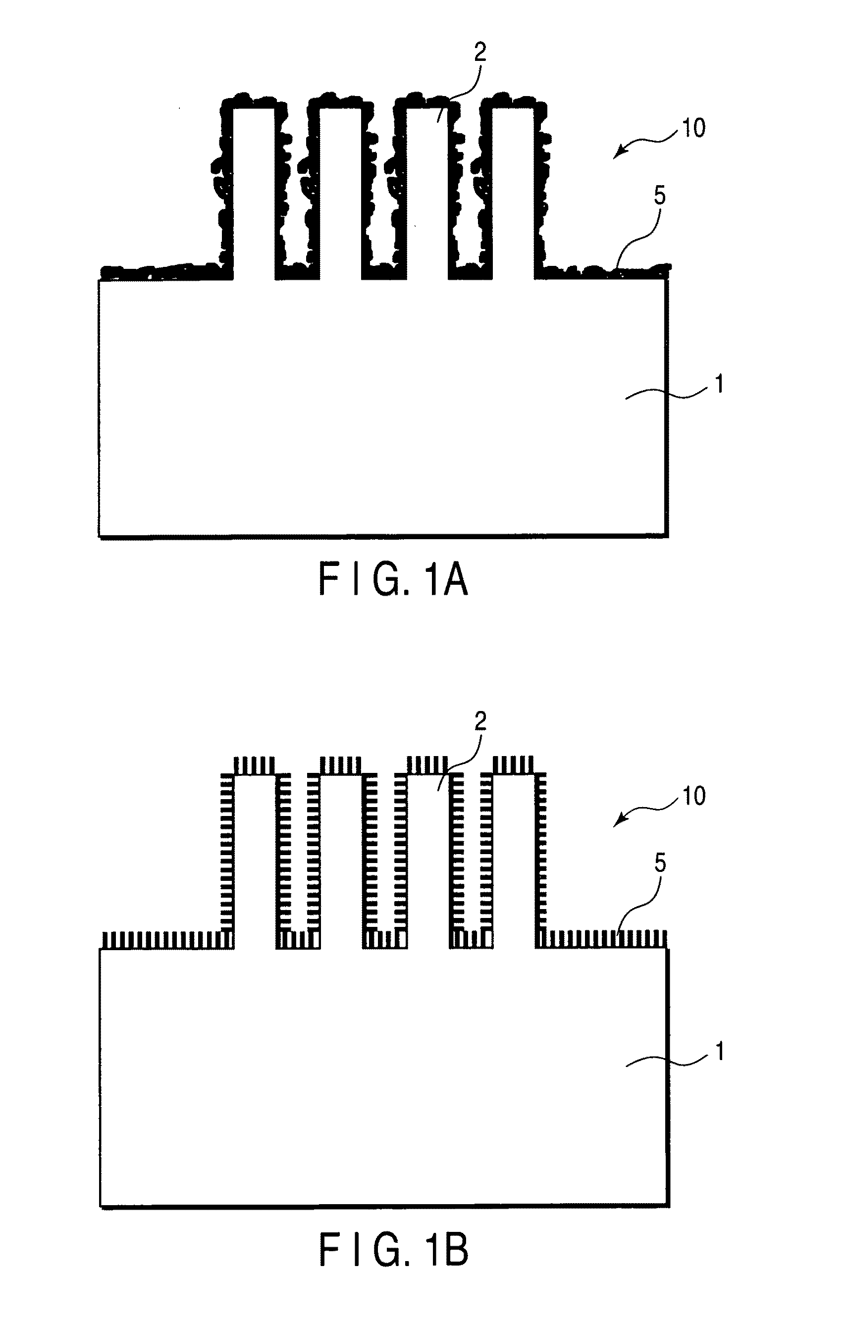
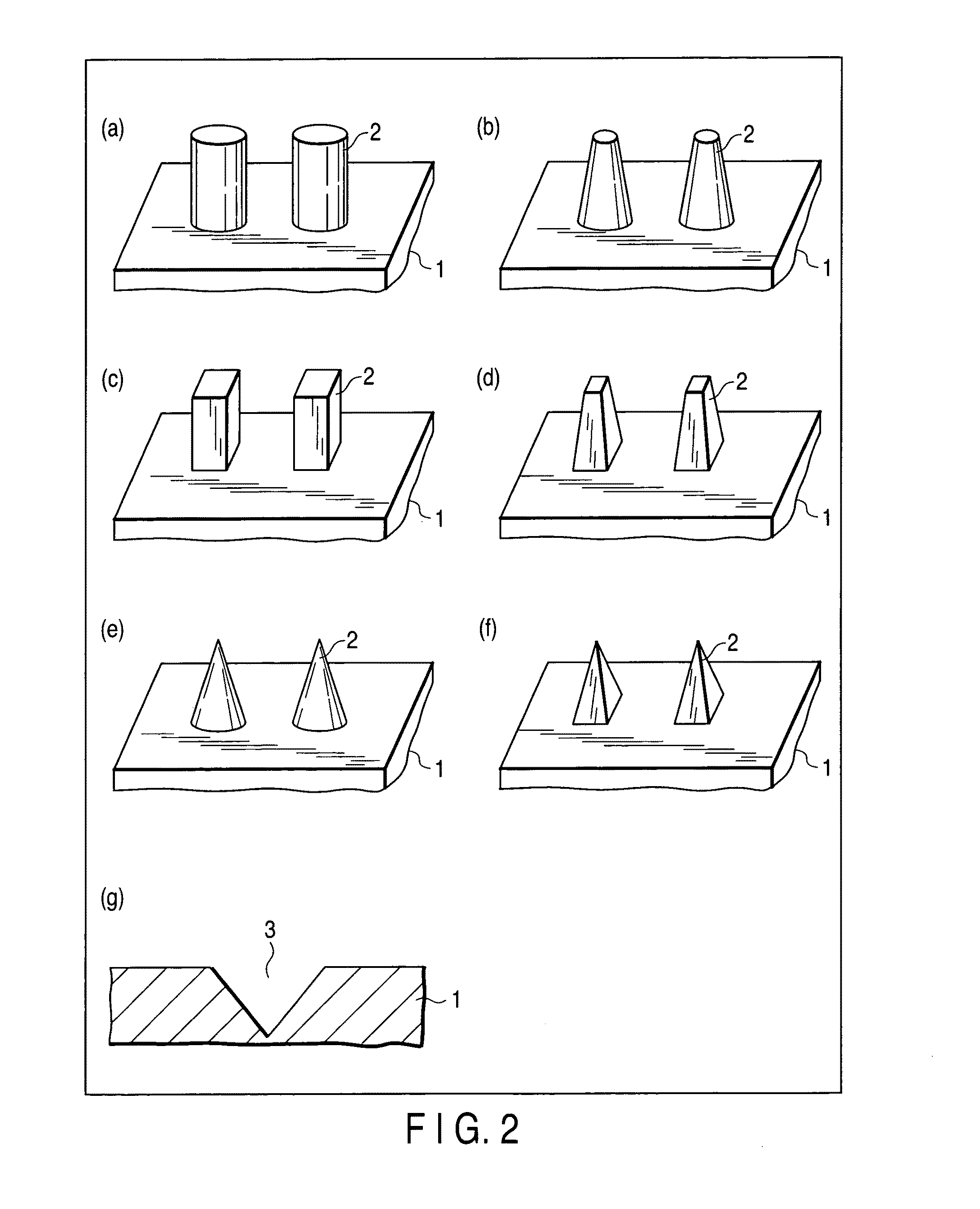
[0067]Mechanical cutting work or chemical etching was applied to the surface of an n-type monocrystalline silicon (100) substrate of low electrical resistance, thereby forming projected portions of square columns or square pyramids on the surface of the substrate.

[0068]Then, by means of sputtering, cobalt employed as a catalyst was deposited to a thickness of 6 nm on the surface of the substrate and the deposited layer was subjected to heat treatment for 10 minutes in air atmosphere at a temperature of 900° C.

[0069]The resultant substrate was immersed in methanol and an electric current was passed through electrodes to the substrate so as to heat the substrate for three minutes at 600° C. at first and then to heat the substrate for 6 minutes at 900° C. As a result, a solid / liquid interface contact decomposition reaction using carbon atoms in the methanol as a raw material was produced in the vicinity of t...


PUM

PropertyMeasurementUnit
heightaaaaaaaaaa
lengthaaaaaaaaaa
thicknessaaaaaaaaaa

Abstract

Disclosed is a nanocarbon material-composite substrate including a substrate, a three-dimensional structural pattern formed on the substrate, and a nanocarbon material formed on a surface of the substrate, wherein the nanocarbon material is disposed at least on side surfaces of the three-dimensional structural pattern.

Description

CROSS-REFERENCE TO RELATED APPLICATIONS[0001]This is a Continuation Application of PCT Application No. PCT / JP2009 / 067061, filed Sep. 30, 2009, which was published under PCT Article 21(2) in Japanese.[0002]This application is based upon and claims the benefit of priority from prior Japanese Patent Application No. 2008-254823, filed Sep. 30, 2008, the entire contents of which are incorporated herein by reference.BACKGROUND OF THE INVENTION[0003]1. Field of the Invention[0004]The present invention relates to a composite substrate containing a nanocarbon material which is expected to be applicable to a reinforcing material, an electron-emitting element material, an electrode material for batteries, an electromagnetic wave-absorbing material, a catalytic material, an optical material, etc.[0005]2. Description of the Related Art[0006]Since the nanocarbon material has a microstructure of the order of nanometers in size and is constituted by carbon atoms of an sp2 hybridized orbit, the nano...

Claims


Application Information

Patent Timeline
Patent Type & Authority Applications(United States)
IPC IPC(8): C01B31/02B32B3/00B05D1/18B05D3/10B05D3/12B32B9/00B32B3/10B32B3/30B82Y30/00B82Y40/00
CPCC09K11/65Y10T428/24174B82Y30/00B82Y40/00Y10T428/24479C01B31/0246Y10T428/30Y10T428/2457Y10T428/24612C01B32/166C01B32/15
Inventor GAMO, HIDENORIKODAMA, YOSHIHIROTAMURA, AKIRA
Owner TOPPAN PRINTING CO LTD
Why Eureka
Try Eureka