Mask blank, mask blank manufacturing method, transfer mask, and transfer mask manufacturing method
a mask manufacturing method and mask technology, applied in the field of mask blanks, mask blank manufacturing methods, transfer masks, and transfer mask manufacturing methods, can solve the problems of affecting the lead time in the production line, affecting the efficiency of the production line, and increasing the cost of repetitive processes
Active Publication Date: 2011-07-28
HOYA CORP
View PDF0 Cites 8 Cited by
- Summary
- Abstract
- Description
- Claims
- Application Information
AI Technical Summary
Benefits of technology
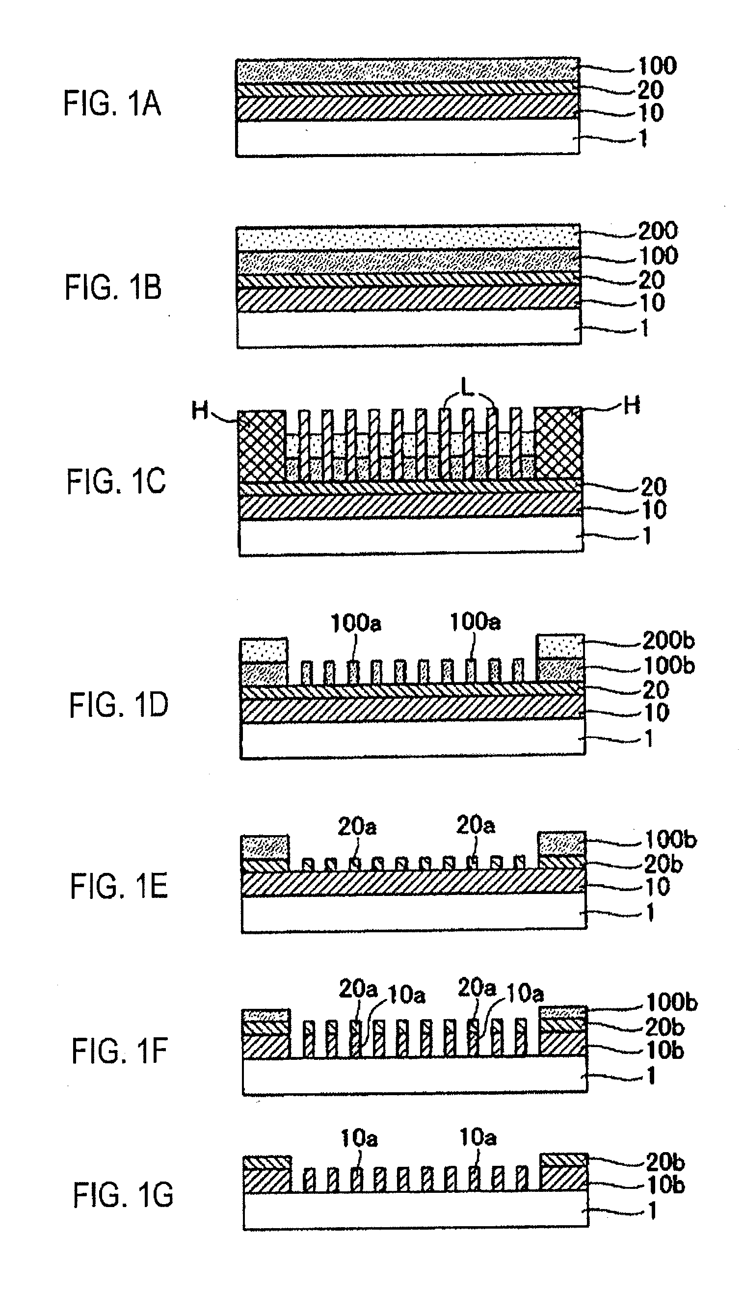
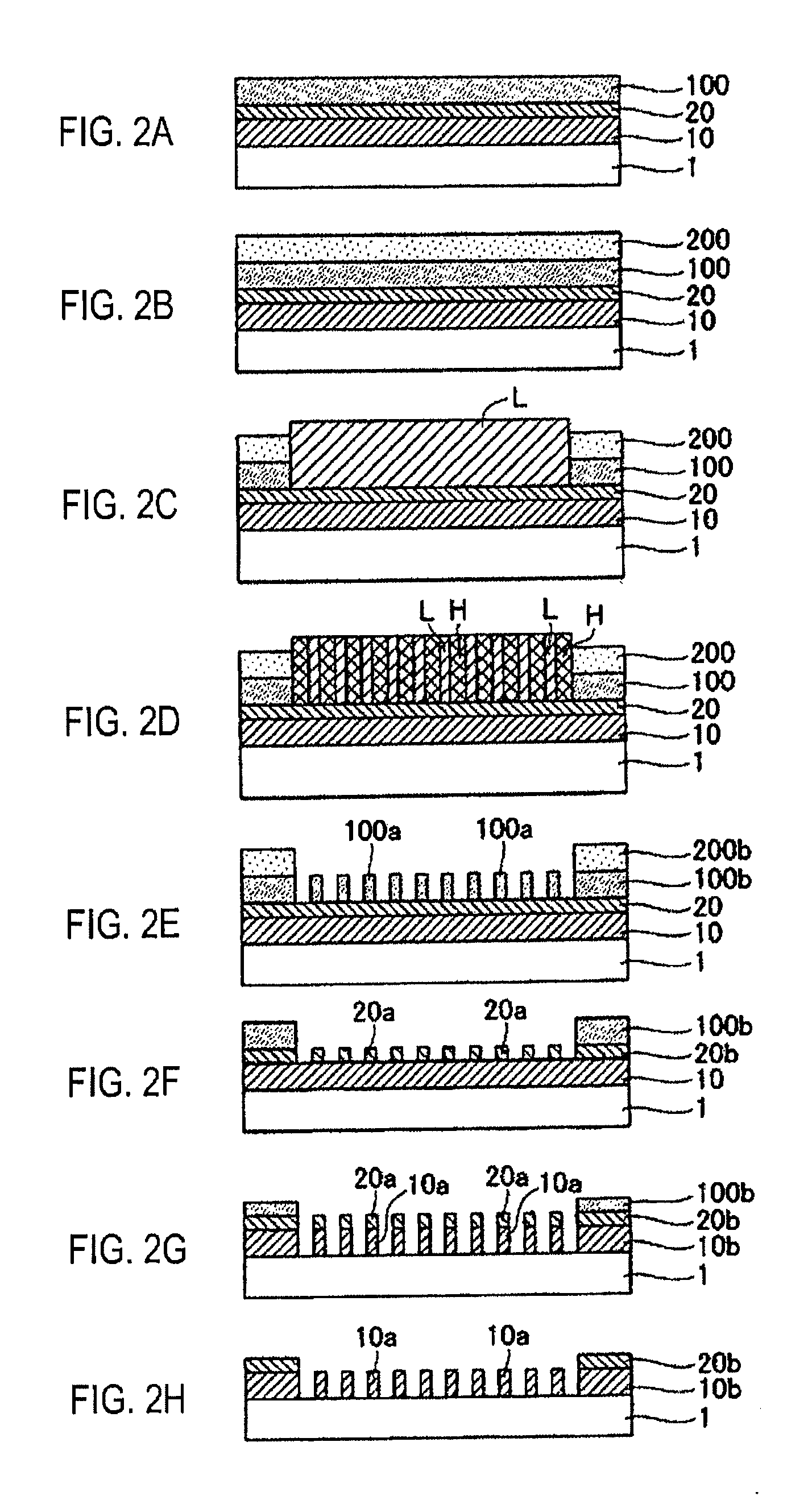
According to one aspect of the present disclosure, a 3-dimensional resist pattern may be formed by one-time writing. Therefore, it is possible to reduce the mask manufacturing process in comparison with a mask manufacturing method performing the applying, writing, developing, and stripping of a resist two times. Further, it is possible to realize the decrease in a fabrication time and in cost. Moreover, it is possible to increase mask fabrication accuracy since the one-time writing can effectively prevent a writing position misalignment, which may be induced from the mask manufacturing method performing the applying, writing, developing, and stripping of a resist two times.
According to still another aspect of the present disclosure, it is possible to realize a manufacturing method for preventing the upper resist pattern from being partially or entirely removed along with the middle layer underneath the upper resist pattern.
Problems solved by technology
Therefore, the repetitive processes are time-consuming and labor intensive increasing cost.
Specifically, if the second resist film is exposed using an electron beam writing apparatus, fabrication time is dramatically increased thereby affecting the lead time in a production line.
The manufacturing process, however, does not fully satisfy the abovementioned accuracy requirements.
Such problem occurs during not only the manufacture of the halftone phase shift mask with the light-shielding band but also the manufacture of a 3-dimensional mask with different fabrication depths, such as a patch of a tri-tone phase shift mask or an enhancer mask.
Method used
View moreImage
Smart ImageViewing Examples
Examples
embodiment 1
(1) Embodiment 1 Lower resist film: a high-sensitivity negative type\Upper resist film: a low-sensitivity negative type (Structure 1) (for example, See FIGS. 1A to 1G and FIGS. 4A to 4G) (corresponding to Configuration 2)
embodiment 2
(2) Embodiment 2 Lower resist film: a low-sensitivity positive type\Upper resist film: a high-sensitivity positive type (Structure 2) (for example, See FIGS. 2A to 2H and FIGS. 5A to 5G) (corresponding to Configuration 3)
embodiment 3
(3) Embodiment 3 Lower resist film: a low-sensitivity positive type\Upper resist film: a high-sensitivity negative type (Structure 3) (for example, See FIGS. 3A to 3H and FIGS. 6A to 6H) (corresponding to Configuration 4)
Login to View More PUM
 Abstract
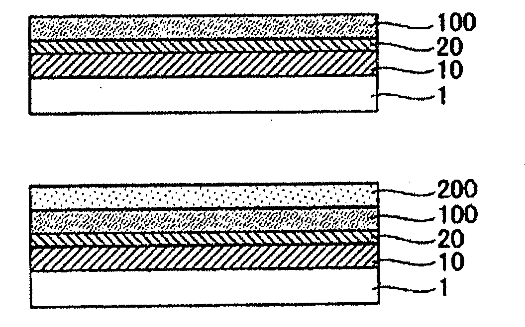
According to certain embodiments, a mask blank for an electron beam writing is provided, capable of forming a resist pattern of a 3-dimensional topology through an one-time writing. The mask blank includes a substrate, a thin film formed on the substrate, and an electron beam resist film formed on the thin film. The electron beam resist film is made of a laminated film including at least a lower resist film and an upper resist film. The lower resist film and the upper resist film have different resist sensitivities with respect to an electron beam.
Description
CROSS-REFERENCE TO RELATED APPLICATIONSThis application is based upon and claims the benefit of priority from Japanese Patent Application No. 2009-289043, filed on Dec. 21, 2009, the entire contents of which is incorporated herein by reference.TECHNICAL FIELDEmbodiments described herein relate generally to a mask blank, a mask blank manufacturing method, a transfer mask, and a transfer mask manufacturing method.BACKGROUNDIn general, during a manufacturing process of a semiconductor device, fine patterns are formed by using photolithography. During the formation of the fine patterns, several substrates, referred to as transfer masks (e.g., photomasks), are used. Such transfer masks are fabricated by forming fine patterns having metal thin films and the like on a transparent glass substrate. Photolithography is also used in the manufacturing process of the transfer mask.As a kind of the transfer mask, a halftone phase shift mask is known in addition to a binary mask with a light-shiel...
Claims
Login to View More Application Information
Patent Timeline
 IPC IPC(8): G03F1/00G03F1/50G03F1/68H01L21/027
CPCG03F7/2063G03F1/32H01L21/0274H01L21/0337
Inventor HASHIMOTO, MASAHIROSHIROTORI, HIROSHIHONMA, YUUSUKESHIRAKURA, MITSUHIRO
Owner HOYA CORP


