Method for reducing pattern collapse in high aspect ratio nanostructures

Active Publication Date: 2011-08-04
LAM RES CORP
View PDF19 Cites 45 Cited by
  • Summary
  • Abstract
  • Description
  • Claims
  • Application Information

AI Technical Summary

Benefits of technology

[0007]To achieve the foregoing and in accordance with the purpose of the present invention, a method of processing a wafer used in fabricating semiconductor devices is provided. The method teaches processing the wafer in such a way as to reduce or eliminate collapse of high aspect ra

Problems solved by technology

Semiconductor devices are fabricated using a long complex procedure.
Hence, as device features shrink on a wafer and as much li

Method used


Image

  • Method for reducing pattern collapse in high aspect ratio nanostructures
  • Method for reducing pattern collapse in high aspect ratio nanostructures
  • Method for reducing pattern collapse in high aspect ratio nanostructures

Examples


Example

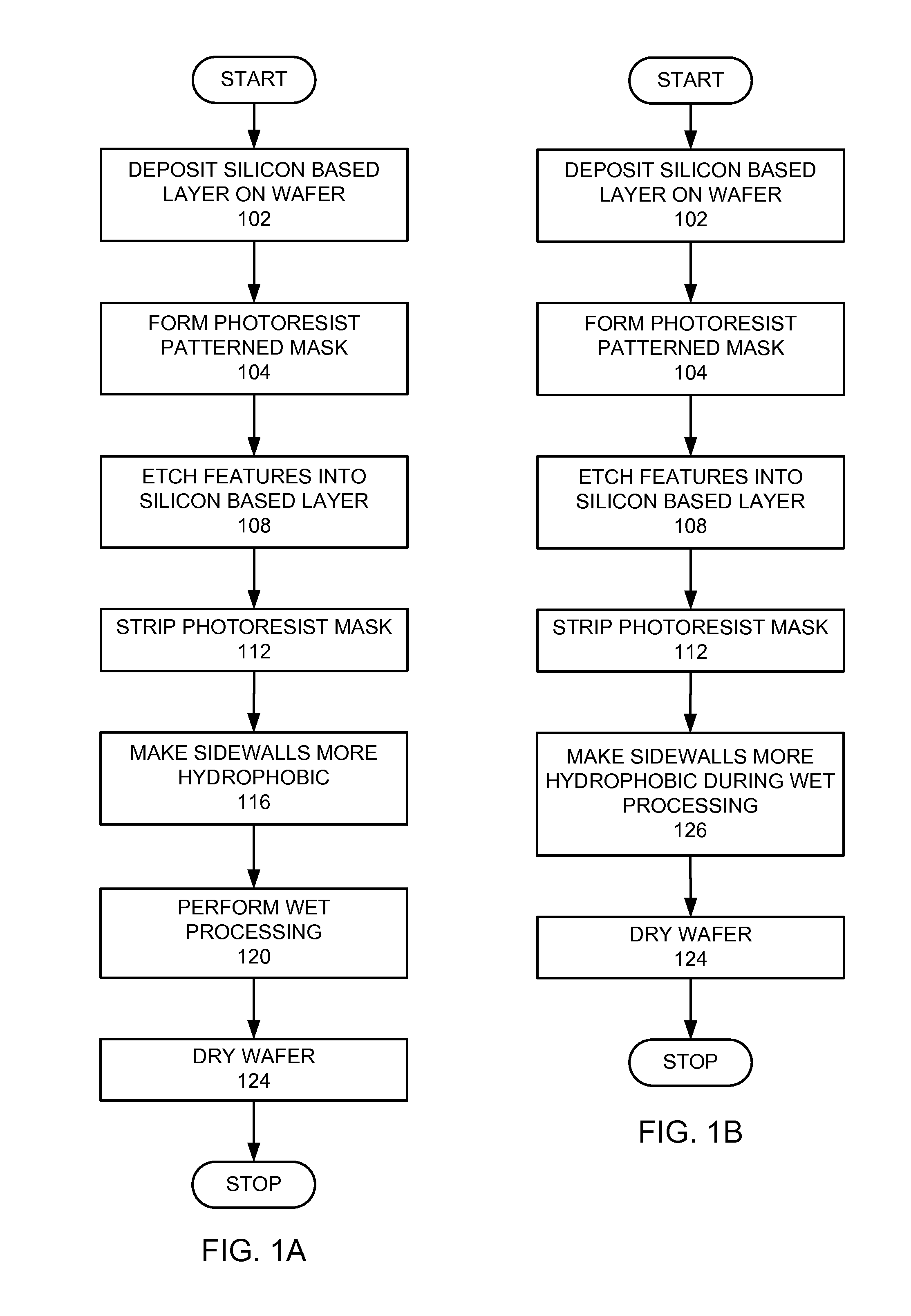
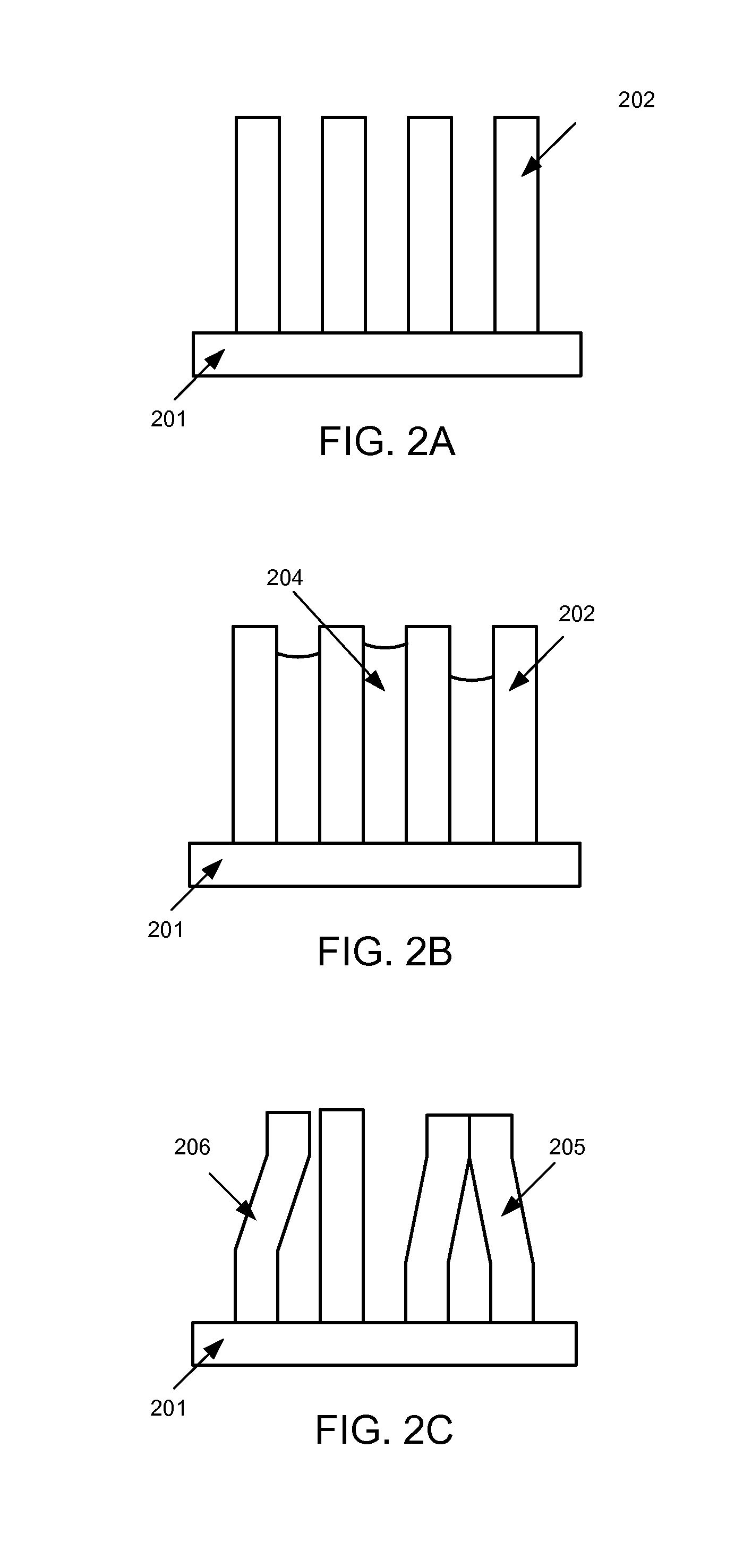
[0016]The present invention will now be described in detail with reference to a few preferred embodiments thereof as illustrated in the accompanying drawings. In the following description, numerous specific details are set forth in order to provide a thorough understanding of the present invention. It will be apparent, however, to one skilled in the art, that the present invention may be practiced without some or all of these specific details. In other instances, well known process steps and / or structures have not been described in detail in order to not unnecessarily obscure the present invention.

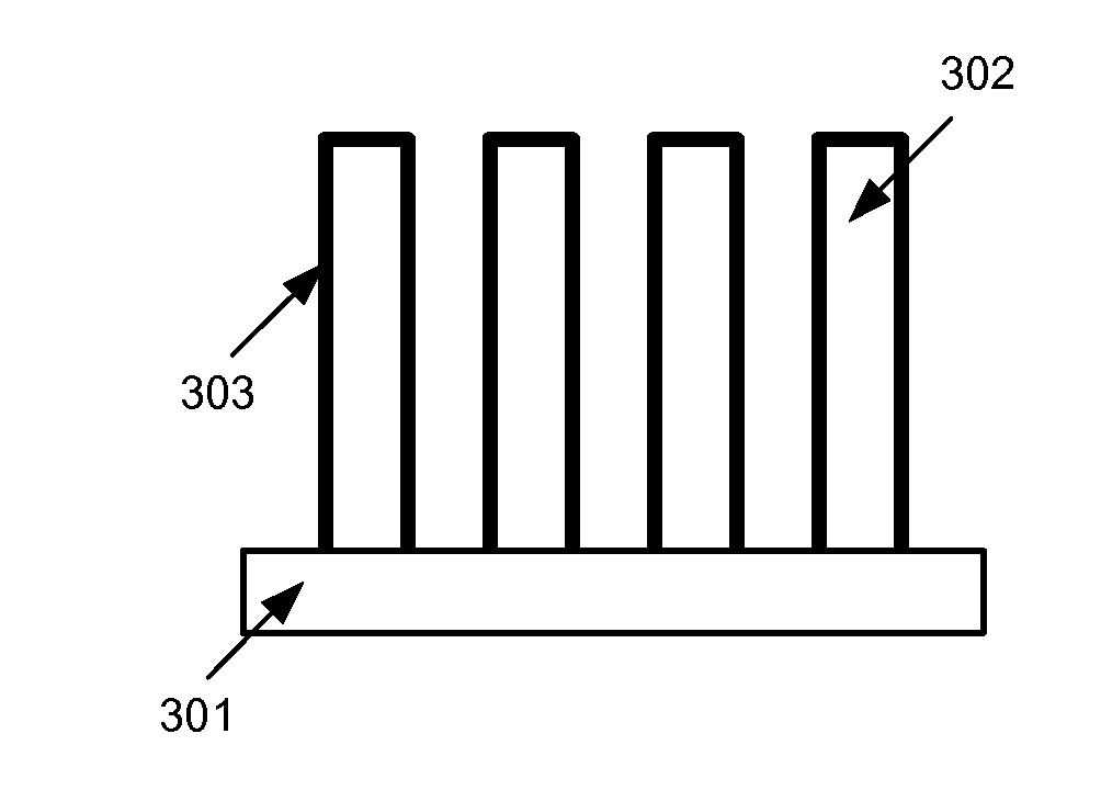
[0017]Oxides and nitrides of silicon grown by low-temperature oxidation (LTO), chemical vapor deposition (CVD) and implantation have been traditionally used in front-end-of-the-line (FEOL) processing for electrical and thermal isolation, masking and encapsulation in high aspect ratio nanostructures. The use of such materials in FEOL applications has continued to offer the selectivity to re...


PUM

PropertyMeasurementUnit
Percent by massaaaaaaaaaa
Weightaaaaaaaaaa
Hydrophobicityaaaaaaaaaa

Abstract

A method is provided for treating the surface of high aspect ratio nanostructures to help protect the delicate nanostructures during some of the rigorous processing involved in fabrication of semiconductor devices. A wafer containing high aspect ratio nanostructures is treated to make the surfaces of the nanostructures more hydrophobic. The treatment may include the application of a primer that chemically alters the surfaces of the nanostructures preventing them from getting damaged during subsequent wet clean processes. The wafer may then be further processed, for example a wet cleaning process followed by a drying process. The increased hydrophobicity of the nanostructures helps to reduce or prevent collapse of the nanostructures.

Description

BACKGROUND OF THE INVENTION[0001]1. Field of the Invention[0002]The invention relates to semiconductor devices. More specifically, the present invention relates to the production of semiconductor devices where wet chemical treatments are used on a wafer with high aspect ratio nanostructures that are sensitive to pattern collapse during processing.[0003]2. Description of the Related Art[0004]Semiconductor devices are fabricated using a long complex procedure. One portion of the procedure involves etching features into a stack of materials on a silicon wafer. The stack of materials may comprise a single layer of silicon based material such as SiO or SiN, or the stack may comprise multiple layers of materials such as SiO, SiN, TEOS, polysilicon or silicon in different orders within the stack. The stack may be formed by a number of methods, including physical vapor deposition, chemical vapor deposition, electrochemical deposition and molecular beam epitaxy, for example. Once the stack o...

Claims


Application Information

Patent Timeline
IPC IPC(8): H01L21/30
CPCH01L21/02057H01L21/02046H01L21/02052H01L21/02054H01L21/02282H01L21/0337
Inventor YASSERI, AMIR A.ZHU, JIYUN, SEOKMINMUI, DAVID S.L.MIKHAYLICHENKO, KATRINA
Owner LAM RES CORP
Why Eureka
Try Eureka