Semiconductor device, chip-on-chip mounting structure, method of manufacturing the semiconductor device, and method of forming the chip-on-chip mounting structure

a semiconductor device and mounting structure technology, applied in the direction of semiconductor devices, semiconductor/solid-state device details, electrical devices, etc., to achieve the effects of preventing short-circuit, preventing electromigration, and enhancing yield and reliability of bonding

Inactive Publication Date: 2011-08-11
SONY CORP
View PDF37 Cites 18 Cited by
  • Summary
  • Abstract
  • Description
  • Claims
  • Application Information

AI Technical Summary

Benefits of technology

[0035]However, according to the present invention, the exposed surface including the side surface of the base metal layer (corresponding to the UBM layer) is covered with the solder bump electrode described above. Thus, in particular, in the Chip-on-Chip mounting carried out in the fluxless fashion, the amount of solder running over in the transverse direction (amount of protrusion) decreases by the amount of the melted solder of the solder bump electrode adhered to the side surface of the base metal layer. Also, the solder bump electrodes disposed adjacent and close to each other in the semiconductor device are prevented from contacting each other, and thus even when the oxide film of the solder surface smashes due to the pressure in a phase of bulging caused by the application of the pressure, it is possible to prevent the short-circuit from being generated between the adjacent solder bump electrodes. As a result, even when the interval between the adjacent solder bump electrodes is reduced, the yield and reliability of the bonding are enhanced.
[0036]In addition, when the underfill material is filled in the space defined between both the semiconductor devices joined to each other, since the amount of solders each running over of the solder bump electrodes is reduced, a thickness of the underfill material between the adjacent solder bump electrodes increases accordingly. As a result, the elements (especially, Sn atoms) composing the solder become difficult to move between the adjacent solder bump electrodes through the underfill material. Thus, it is possible to prevent the electromigration from being generated, and it is also possible to increase the margin of the interval and disposition between the adjacent solder bump electrodes.

Problems solved by technology

As a result, electromigration is generated such that Sn atoms move between the adjacent solder bump electrodes through fine pores in the underfill material, and also causes the short-circuit.

Method used


Image

  • Semiconductor device, chip-on-chip mounting structure, method of manufacturing the semiconductor device, and method of forming the chip-on-chip mounting structure
  • Semiconductor device, chip-on-chip mounting structure, method of manufacturing the semiconductor device, and method of forming the chip-on-chip mounting structure
  • Semiconductor device, chip-on-chip mounting structure, method of manufacturing the semiconductor device, and method of forming the chip-on-chip mounting structure

Examples


first embodiment

1. First Embodiment

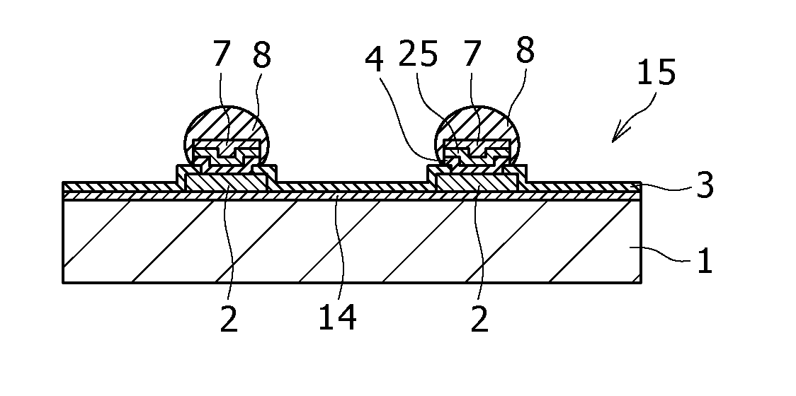
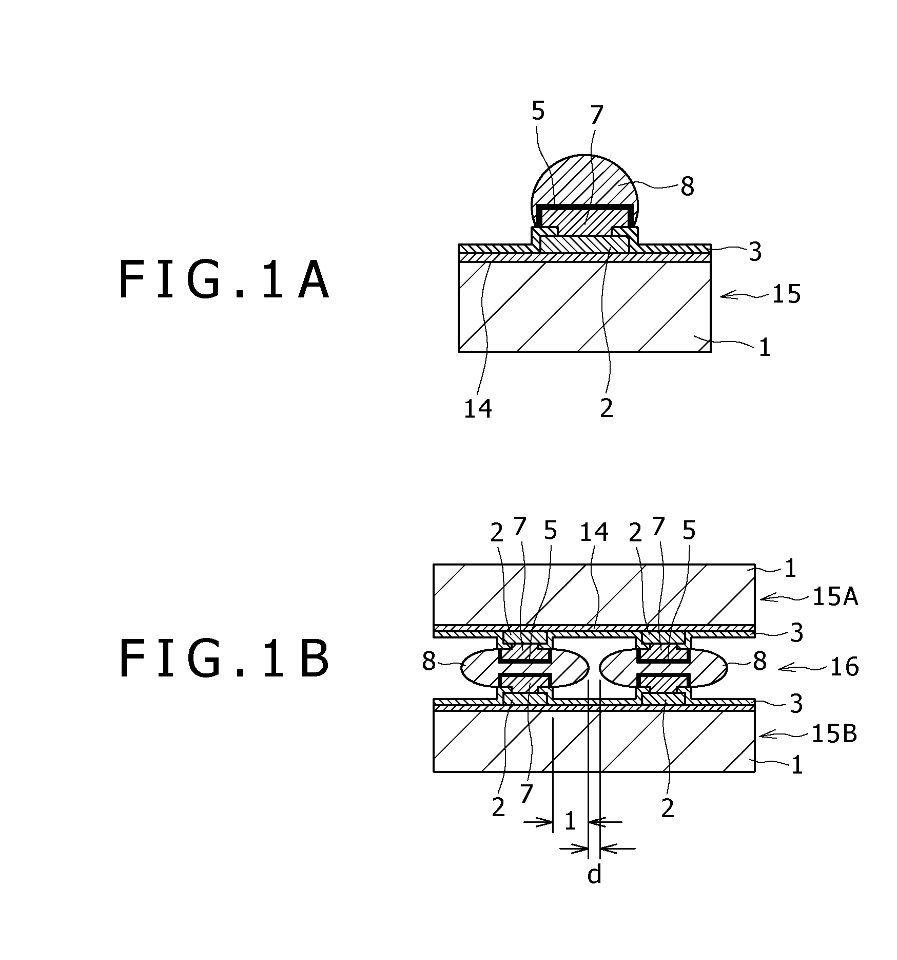
[0051]FIGS. 1A and 1B schematically show a structure of a semiconductor device (semiconductor chip) 15 according to a first embodiment of the present invention.

[0052]The semiconductor device 15 is composed of a semiconductor substrate 1 made of Si or the like, a pad electrode 2 made of aluminum, an insulating film 14 (corresponding to the insulating film 64 previously stated in the related art), a protective film 3 (corresponding to the protective film 64 previously stated in the related art), a copper (Cu) electrolytic plating layer 5, a Ni electrolytic plating layer 7, a Sn system solder bump electrode 8, and the like. Also, an Under Bump Metal (UBM) layer is composed of the Ni electrolytic plating layer 7 and also the Cu electrolytic plating layer 5. A size of the solder bump electrode 8, for example, may be equal to or smaller than 30 μm in diameter and equal to or smaller than 15 μm in height.

[0053]As shown in FIG. 1A, it is important for the semiconductor de...

second embodiment

2. Second Embodiment

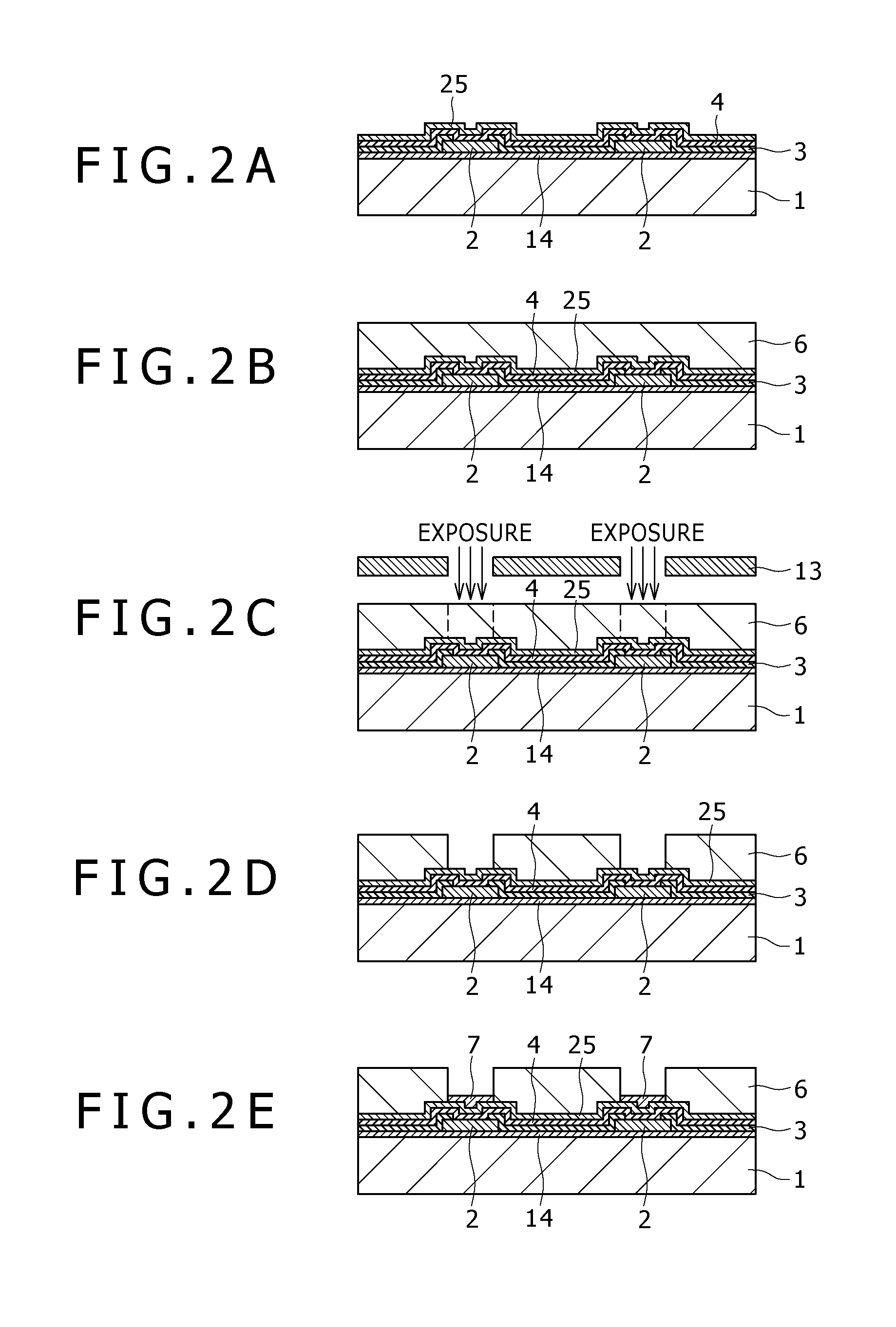
[0071]FIGS. 3A to 3I show a semiconductor device according to a second embodiment of the present invention, and processes for manufacturing the semiconductor device of the second embodiment, respectively.

[0072]Firstly, similarly to the case of the description given with reference to FIGS. 4A to 4H, the insulating film 14, the pad electrode 2, the protective film 3, the Ti sputtering layer 4, the Cu sputtering layer 25, and the Ni electrolytic plating layer 7 are formed in this order on the semiconductor substrate 1.

[0073]Next, as shown in FIG. 3B, the Cu sputtering layer 25 is selectively etched away with the Ni electrolytic plating layer 7 as an etching mask except for a portion of the Cu sputtering layer 25 underlying the Ni electrolytic plating layer 7.

[0074]Next, as shown in FIG. 3C, the Ti sputtering layer 4 is selectively etched away with the Ni electrolytic plating layer 7 as an etching mask except for a portion of the Ti sputtering layer 4 underlying the ...


PUM


Abstract

A semiconductor device includes: a semiconductor chip having a semiconductor substrate; a pad electrode formed on the semiconductor substrate; a base metal layer formed on said pad electrode; and a bump electrode formed on the base metal layer, in which an exposed surface including a side surface of the base metal layer is covered with the solder bump electrode.

Description

BACKGROUND OF THE INVENTION[0001]1. Field of the Invention[0002]The present invention relates to a semiconductor device suitable for manufacturing an electronic apparatus, a Chip-on-Chip mounting structure using the semiconductor device, a method of manufacturing the semiconductor device, and a method of forming the Chip-on-Chip mounting structure using the semiconductor device.[0003]2. Description of the Related Art[0004]Heretofore, a semiconductor device having solder bump electrodes has been used as a key part of electronic apparatuses such as video equipment such as a television receiver, audio equipment, a mobile phone, and a personal computer.[0005]FIGS. 4A to 4O show processes for manufacturing a semiconductor chip as a semiconductor device 65, respectively. These manufacturing processes, for example, are disclosed in “Introduction of CASIO solder BUMP technology (Smart & Fine Technologies)” which will be described later.[0006]Firstly, as shown in FIG. 4A, an insulating film ...

Claims


Application Information

Patent Timeline
Patent Type & Authority Applications(United States)
IPC IPC(8): H01L23/498H01L21/60
CPCH01L23/3114H01L24/05H01L2924/0002H01L2224/0401H01L2924/0105H01L2924/01019H01L2924/01006H01L2924/01005H01L2224/131H01L2924/3841H01L2924/014H01L2924/01078H01L2924/01047H01L2924/01046H01L2924/01033H01L24/11H01L24/13H01L25/0657H01L25/50H01L2224/0346H01L2224/0347H01L2224/05022H01L2224/05027H01L2224/05124H01L2224/05155H01L2224/05166H01L2224/05562H01L2224/05647H01L2224/1146H01L2224/1147H01L2224/1181H01L2224/11849H01L2224/11912H01L2224/13023H01L2224/13111H01L2224/81097H01L2225/06513H01L2924/01013H01L2924/01029H01L2924/0103H01L2924/00014H01L2924/01014H01L2224/05552
Inventor OZAKI, HIROSHIASAMI, HIROSHI
Owner SONY CORP
Why Eureka
Try Eureka