Multilayer Wiring Substrate, and Method of Manufacturing the Same

a multi-layer wiring and substrate technology, applied in the direction of resist details, printed circuit aspects, printed circuit manufacturing, etc., can solve the problem of increasing the manufacturing cost of multi-layer wiring substrate, and achieve the effect of reducing the possibility of crack generation in the resin insulation layer and increasing the strength of solder connection

Inactive Publication Date: 2011-08-18
NGK SPARK PLUG CO LTD
View PDF36 Cites 30 Cited by
  • Summary
  • Abstract
  • Description
  • Claims
  • Application Information

AI Technical Summary

Benefits of technology

[0025]According to the aspect mentioned above, the second-main-surface-side connection terminals can be reliably formed such that a peripheral portion of the terminal outer surface of each second-main-surface-side connection terminal is covered by the corresponding outermost resin insulation layer. Moreover, the concave portion is formed on the terminal outer surface of each second-main-surface-side connection terminal such that the deepest portion of the concave portion is located on the inner layer side in relation to the peripheral portion of the terminal outer surface. When the second-main-surface-side connection terminals are formed in this manner, the stress acting at the boundary between each second-main-surface-side connection terminal and the corresponding resin insulation layer can be mitigated, whereby the possibility of generation of cracks in the resin insulation layer decreases. Furthermore, since the area of contact between solder and the terminal outer surface increases, the strength of solder connection can be increased. Moreover, in the manufacturing method of the present invention, since the second-main-surface-side connection terminals are not required to be formed in a predetermined pattern after the build-up step, the multilayer wiring substrate can be manufactured relatively easily.
[0026]The step of forming openings in the outermost resin insulating layer may be performed after the step of laminating on the metal foil a build-up material, and may include a step of performing laser drilling on the outermost resin insulation layer on the second main surface side to thereby form the openings, the openings for exposing portions of the metal foil. The method may further include, after the step of performing laser drilling, a step of forming a plating resist film on the outermost resin insulation layer on the second main surface, and a step of forming, at positions corresponding to the openings, additional openings in the plating resist film which are greater in area than the openings. The step of forming the metal conductor portion may be performed after the steps of forming a plating resist film and forming additional openings, and may further include: a step of performing electro plating so as to form the metal conductor portions in each of the openings and the additional openings; and a step of removing the plating resist film. In this case, the metal conductor portions, which are to be used as the second-main-surface-side connection terminals, can be formed reliably.

Problems solved by technology

In this case, since a structure (e.g., a reinforcing plate or the like) is additionally required so as to restrain the warpage, the manufacturing cost of the multilayer wiring substrate increases.

Method used


Image

  • Multilayer Wiring Substrate, and Method of Manufacturing the Same
  • Multilayer Wiring Substrate, and Method of Manufacturing the Same
  • Multilayer Wiring Substrate, and Method of Manufacturing the Same

Examples


first embodiment

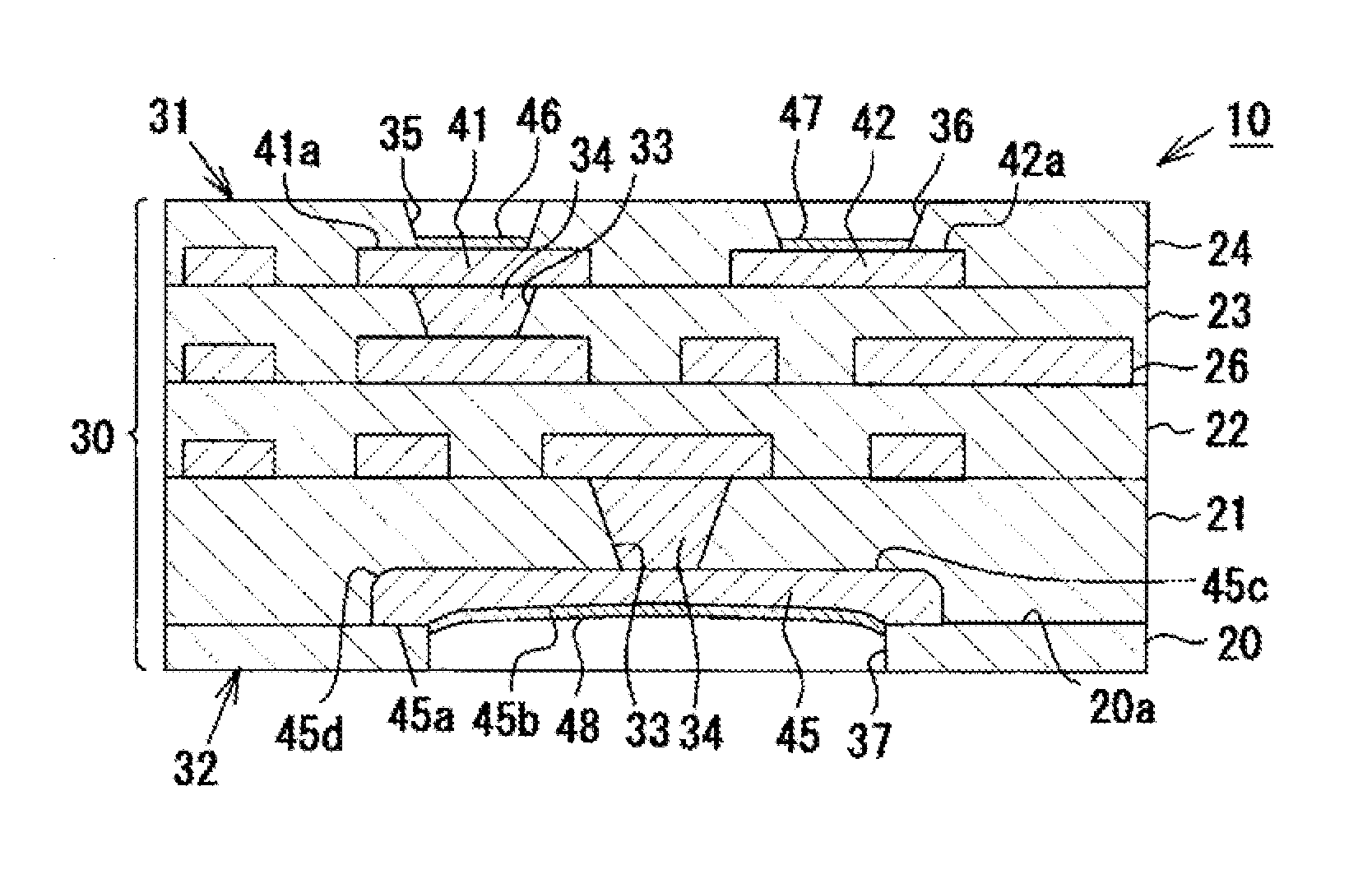
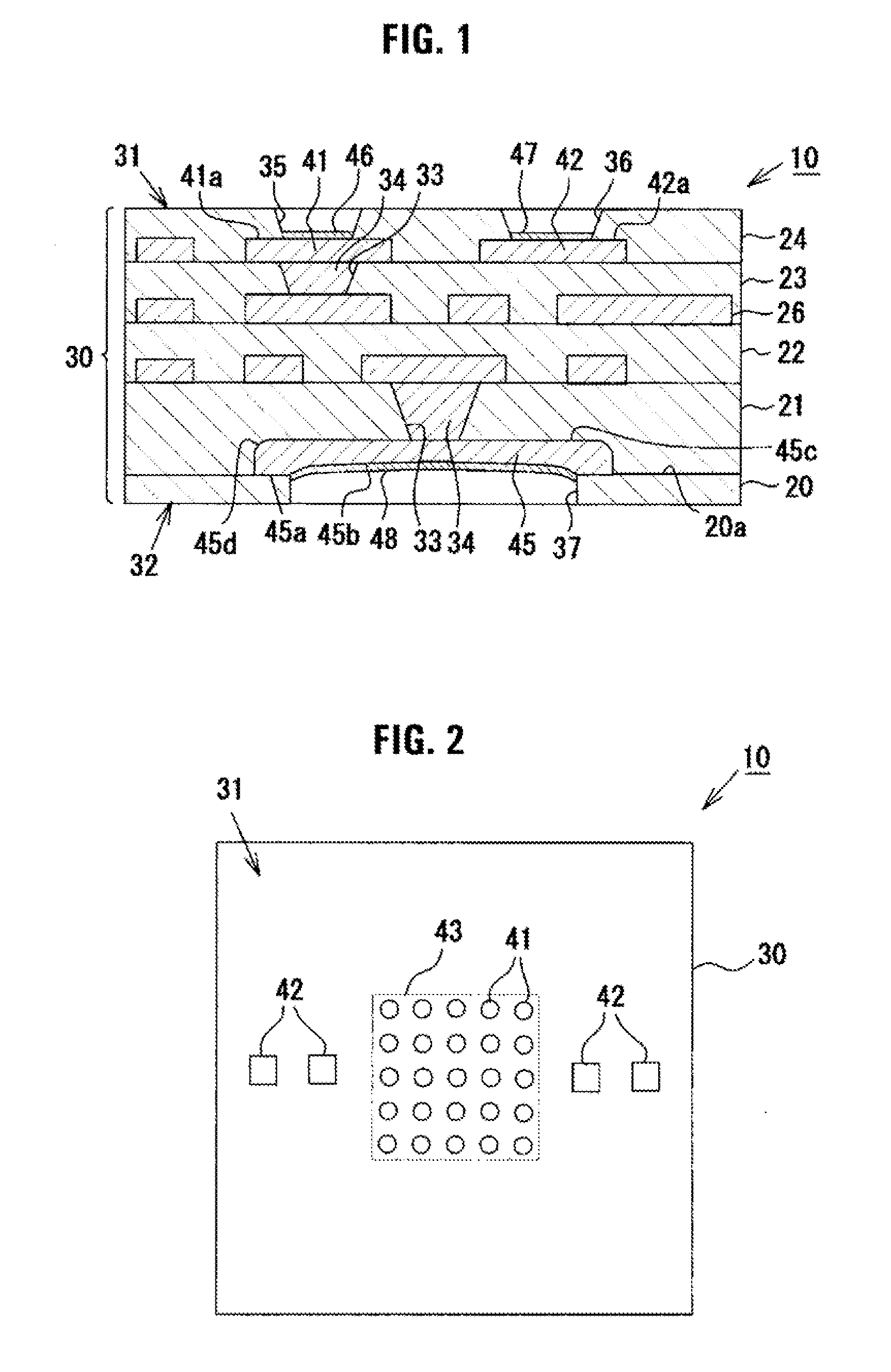
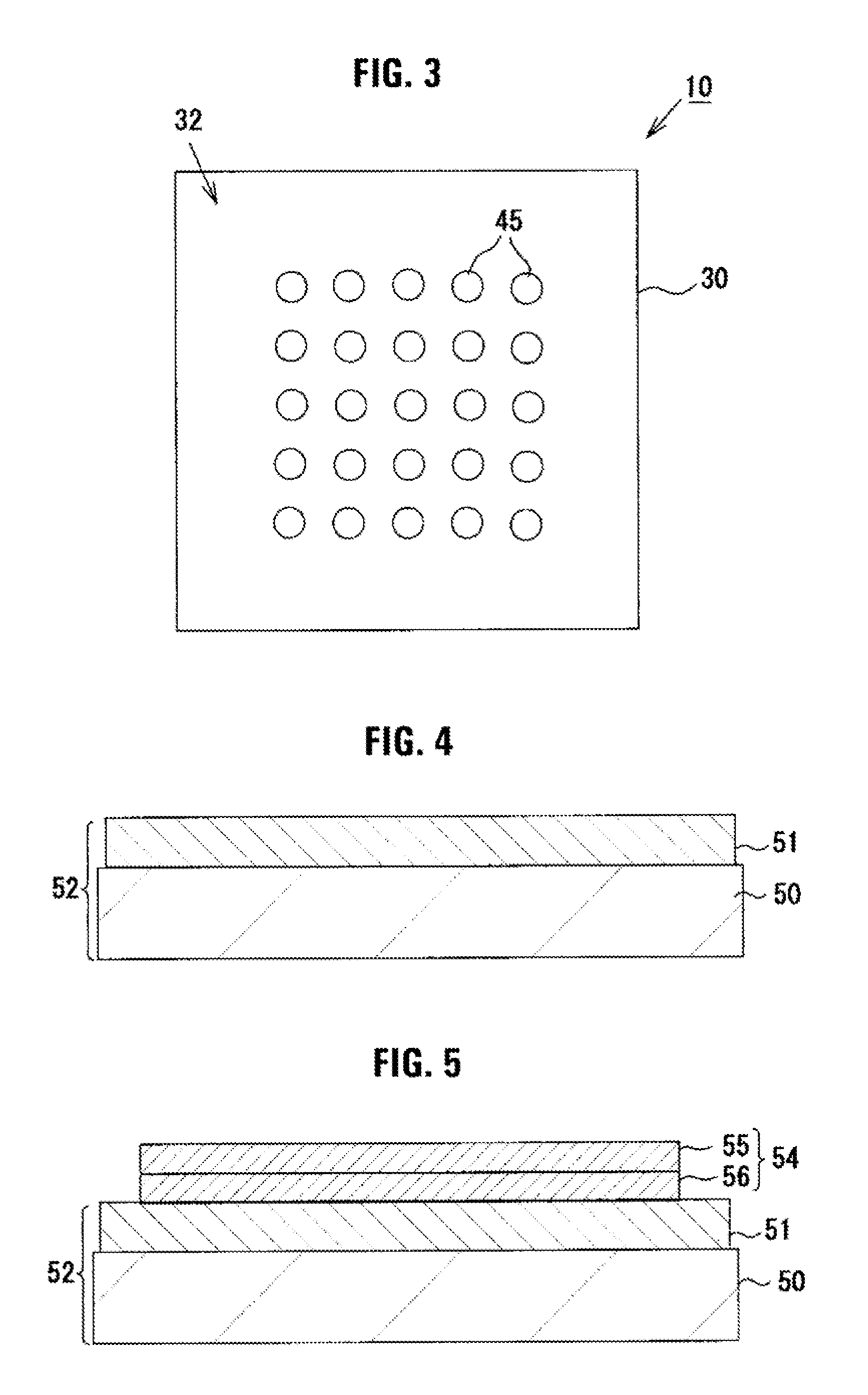
[0057]A multilayer wiring substrate according to a first embodiment of the present invention will next be described in detail with reference to the drawings. FIG. 1 is an enlarged sectional view schematically showing the structure of the multilayer wiring substrate of the present embodiment. FIG. 2 is a plan view of the multilayer wiring substrate as viewed from the top surface side. FIG. 3 is a plan view of the multilayer wiring substrate as viewed from the bottom surface side.

[0058]As shown in FIG. 1, a multilayer wiring substrate 10 is a coreless wiring substrate having no substrate core and has a multilayer wiring laminate portion 30 (laminate structure) in which a plurality of resin insulation layers 20, 21, 22, 23, and 24 made primarily of the same resin insulation material, and a plurality of conductive layers 26 made of copper are laminated alternately. The resin insulation layers 20 to 24 are formed of a build-up material made primarily of a hardened resin insulation materi...

second embodiment

[0095]Next, a second embodiment of the present invention will be described with reference to the drawings. The present embodiment differs from the first embodiment in the insulation-layer / conductor-portion forming step of the method of manufacturing the multilayer wiring substrate 10. Notably, the structure of the multilayer wiring substrate 10 is identical with that of the first embodiment.

[0096]A method of manufacturing the multilayer wiring substrate 10 of the present embodiment will now be described.

[0097]In the insulation-layer / conductor-portion forming step of the present embodiment, each metal conductor portion 58, which is to become a motherboard connection terminal 45, has a lower layer having a small area and an upper layer having a large area, and the lower and upper layers are formed in different steps.

[0098]Specifically, as in the first embodiment, after the base-material preparation step (see FIG. 5), electroless copper plating is performed so as to form a full-surface...


PUM

PropertyMeasurementUnit
conductiveaaaaaaaaaa
diametersaaaaaaaaaa
areaaaaaaaaaaa

Abstract

A plurality of openings are formed in a resin insulation layer on a top surface side of a wiring laminate portion, and a plurality of openings are formed in a resin insulation layer on a bottom surface side thereof. A plurality of connection terminals are disposed to correspond to the openings. Peripheral portions of terminal outer surfaces of the connection terminals are covered by the resin insulation layer on the top surface side, and peripheral portions of terminal outer surfaces of the connection terminals are covered by the resin insulation layer on the bottom surface side. Each of the second-main-surface-side connection terminals has a concave portion at the center of the terminal outer surface, and the deepest portion of the concave portion is located on the interior side in relation to the peripheral portion of the terminal outer surface.

Description

CROSS-REFERENCE TO RELATED APPLICATIONS[0001]The present application claims priority to Japanese Patent Application No. 2010-31864, which was filed on Feb. 16, 2010, the disclosure of which is incorporated by reference in its entirety.BACKGROUND OF THE INVENTION[0002]1. Field of the Invention[0003]The present invention relates to a multilayer wiring substrate having a laminate structure in which a plurality of resin insulation layers made primarily of the same resin insulation material, and a plurality of conductive layers are laminated alternately in multilayer arrangement, and not having a so-called substrate core in a final product, the substrate core carrying build-up layers successively formed on opposite surfaces thereof. The present invention also relates to a method of manufacturing such a multilayer wiring substrate.[0004]2. Description of Related Art[0005]In association with recent increasing tendency toward higher operation speed and higher functionality of semiconductor ...

Claims


Application Information

Patent Timeline
Patent Type & Authority Applications(United States)
IPC IPC(8): H05K1/09H01R43/00H05K1/00
CPCH01L23/49811Y10T29/302H01L23/49827H05K1/113H05K3/205H05K3/4682H05K2201/09745H05K2201/099H05K2203/0361H05K2203/0369H05K2203/0588H01L2924/0002H01L23/49822Y10T29/49117H01L2924/00H01L23/12H05K3/46
Inventor MAEDA, SHINNOSUKESUZUKI, TETSUOHIRANO, SATOSHI
Owner NGK SPARK PLUG CO LTD
Why Eureka
Try Eureka