Sic semiconductor device having cjfet and method for manufacturing the same

a semiconductor device and semiconductor technology, applied in the field of semiconductor devices, can solve the problems of restricted noise propagation at high frequency, high frequency noise is absorbed, and restricted and achieve the effect of reducing current leakage at high temperature and transmission at high frequency

Inactive Publication Date: 2011-08-18
DENSO CORP
View PDF8 Cites 8 Cited by
  • Summary
  • Abstract
  • Description
  • Claims
  • Application Information

AI Technical Summary

Benefits of technology

[0008]In view of the above-described problem, it is an object of the present disclosure to provide a SIC semiconductor device having a CJFET. It is another object of the present disclosure to provide a m

Problems solved by technology

Further, the insulation separation layer is made of an intrinsic SiC layer having the semi-insulating property instead of a PN junction separation, and therefore, high freque

Method used


Image

  • Sic semiconductor device having cjfet and method for manufacturing the same
  • Sic semiconductor device having cjfet and method for manufacturing the same
  • Sic semiconductor device having cjfet and method for manufacturing the same

Examples


first embodiment

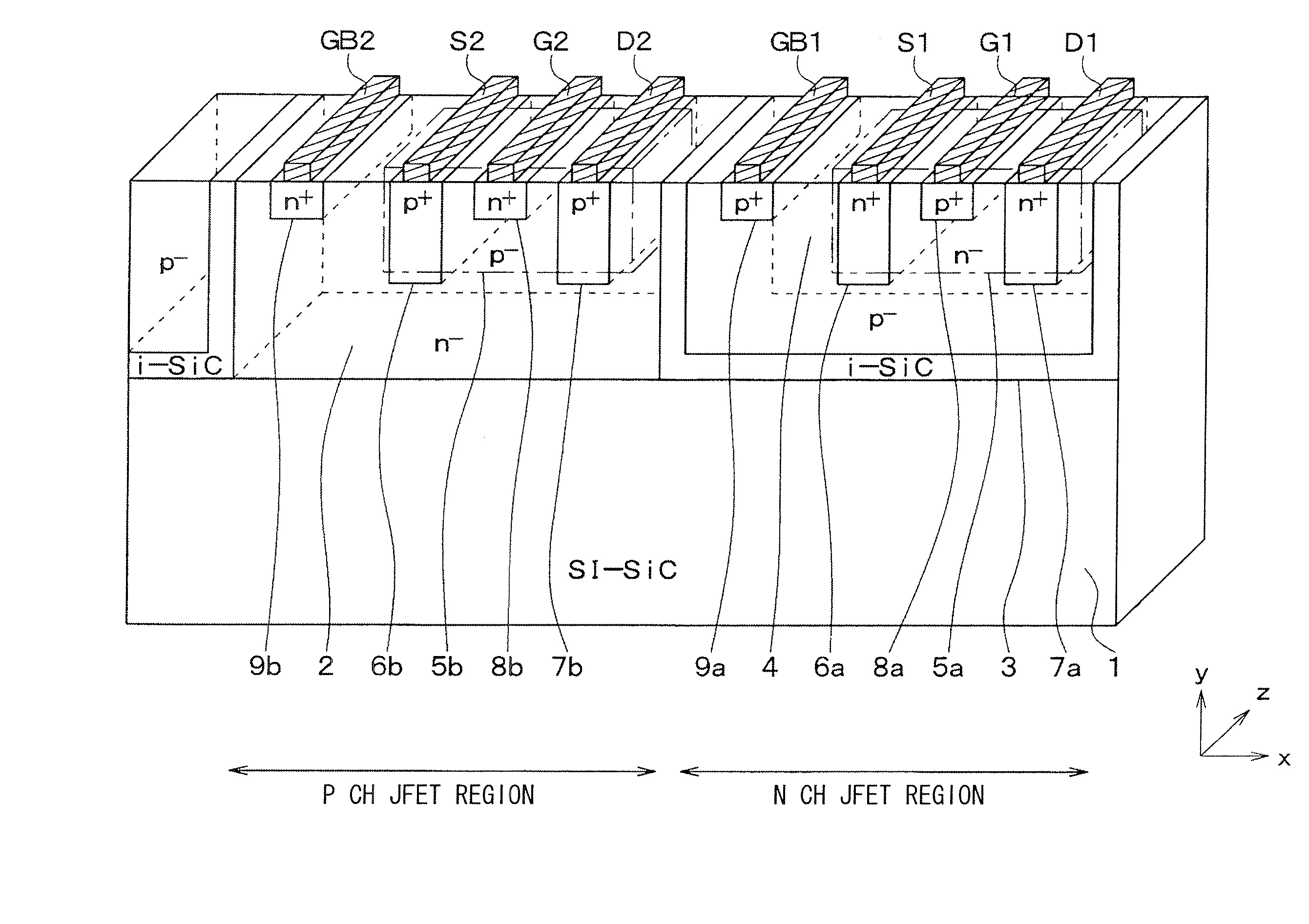
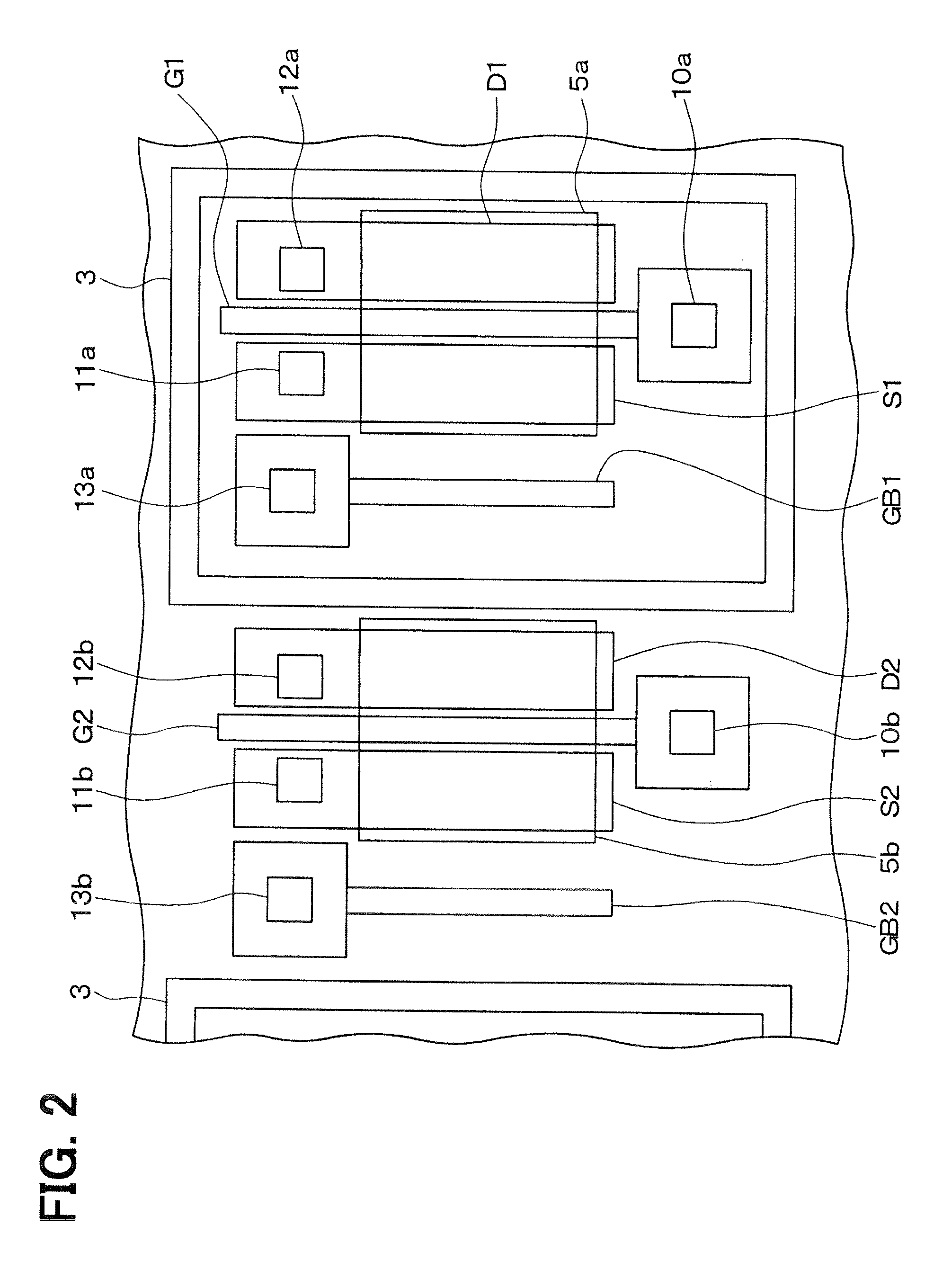
[0027]A SiC semiconductor device according to a first embodiment will be explained. FIG. 1 shows the SiC semiconductor device having a CJFET. FIG. 2 is a layout view of the SiC semiconductor device. A structure of the CJFET in the device will be explained as follows. In FIG. 1, a right-left direction of the drawing is defined as X direction, an up-down direction of the drawing is defined as a Y direction, and a direction perpendicular to the X and Y directions is defined as Z direction.

[0028]The SiC semiconductor device is made of a SiC substrate 1 having semi-insulating property (‘i.e., SI-SiC substrate). The semi-insulating property is provided by a non-doped semiconductor material having resistivity or conductivity near insulation material. For example, in the present embodiment, the SiC substrate 1 having semi-insulating property is an offset substrate made of 4H-SiC. A principal surface of the substrate 1 has an offset angle with respect to a (0001)-Si surface or a (000-1)-C su...

second embodiment

[0068]A second embodiment will be explained. A SiC semiconductor device according to the present embodiment has the first back gate electrode GB1, the first source electrode S1, the second back gate electrode GB2 and the second source electrode S2, which are different from the first embodiment.

[0069]FIG. 13 shows the SiC semiconductor device having the CJFET. As shown in FIG. 13, the first back gate electrode GB1 and the first source electrode S1 are common so that the potential of the first back gate electrode GB1 is fixed to the potential of the first source electrode S1. Further, the second back gate electrode GB2 and the second source electrode S2 are common so that the potential of the second back gate electrode GB2 is fixed to the potential of the second source electrode S2.

[0070]Thus, when the first back gate electrode GB1 and the first source electrode 51 are common, and the second back gate electrode GB2 and the second source electrode S2 are common, the potential of the fi...

third embodiment

[0071]A third embodiment will be explained. A SiC semiconductor device according to the present embodiment has the insulation separation layer 3, which is different from the first embodiment.

[0072]FIG. 14 shows the SiC semiconductor device having the CJFET. As shown in FIG. 14, in the present embodiment, not only the N conductive type SiC layer 2 is formed in the P channel JFET region on the surface of the substrate 1, but also the P conductive type SiC layer 4 is directly formed in the N channel JFET region. The P channel JFET region and the N channel JFET region are separated and insulated from each other with the insulation separation layer 3, which extends along with the vertical direction of the substrate 1. Specifically, in the present embodiment, the insulation separation layer 3 is not arranged to surround the sidewall and the bottom of the P conductive type SiC layer 4, but arranged to be disposed on the sidewall of the P conductive type SiC layer 4. More specifically, the ...


PUM


Abstract

A SiC semiconductor device includes: a SiC substrate made of intrinsic SiC having semi-insulating property; first and second conductive type SiC layers disposed in the substrate; an insulation separation layer made of intrinsic SiC for isolating the first conductive type SiC layer from the second conductive type SiC layer; first and second conductive type channel JFETs disposed in the first and second conductive type SiC layers, respectively. The first and second conductive type channel JFETs provide a complementary junction field effect transistor. Since an electric element is formed on a flat surface, a manufacturing method is simplified. Further, noise propagation at high frequency and current leakage at high temperature are restricted.

Description

CROSS REFERENCE TO RELATED APPLICATION[0001]This application is based on Japanese Patent Application No. 2010-29228 filed on Feb. 12, 2010, the disclosure of which is incorporated herein by reference.FIELD OF THE INVENTION[0002]The present invention relates to a SiC semiconductor device having a CJFET (complementary junction type field effect transistor) and a method for manufacturing a SiC semiconductor device with CJFET.BACKGROUND OF THE INVENTION[0003]Conventionally, a vertical CJFET made of SIC substrate includes a N channel JFET and a P channel JFET. The SiC material has semi-insulating (i.e., SI) property. The CJFET is disclosed in, for example, U.S. Pat. No. 6,503,782 and US 2007 / 0012946. In the CJFET, an impurity layer formed on the SiC substrate is divided by a trench etching method so that the N channel JFET region and the P channel JFET region are separated from each other. Thus, the N channel JFET region is isolated from the P channel JFET region.[0004]Further, a vertica...

Claims


Application Information

Patent Timeline
IPC IPC(8): H01L29/24H01L21/761
CPCH01L21/7602H01L21/8213H01L29/808H01L29/1608H01L29/66068H01L27/098
Inventor MALHAN, RAJESH KUMAR
Owner DENSO CORP
Why Eureka
Try Eureka