Multilayer substrate

a multi-layer substrate and substrate technology, applied in the field of multi-layer substrates, can solve the problems of crosstalk effect between signals via pairs and transformation between differential and common modes, the need for additional space in high-density configurations, and the inability to achieve the effect of preventing leakage losses, reducing the amount of space in layouts, and reducing the number of leakage losses

Inactive Publication Date: 2011-08-25
NEC CORP
View PDF8 Cites 35 Cited by
  • Summary
  • Abstract
  • Description
  • Claims
  • Application Information

AI Technical Summary

Benefits of technology

[0015]To calculate the S-parameters, the finite-difference time-domain method, which is verified as one of the most accurate numerical techniques in world-wide practice, is used. In FIG. 2, the leakage losses calculated according to Eq.1 are presented in the frequency band up to 20 GHz. As follows from this figure, the leakage losses can considerably increase at higher frequencies. This effect means that the transformation of the differential mode to the common mode, radiation from the multilayer PCB, and crosstalk increase at the higher frequencies. To prevent leakage losses, a ground via shielding around a signal via or a signal via pair can be used. However, if a shielding is used around each signal via or differential signal pair, then it can lead to the increase of the space in a layout that is a critical issue in the most of the high-density structures and, moreover, to the increase of the fabrication cost.

Problems solved by technology

However, in this case, a problem of a deficit of space for an appropriate arrangement of ground vias around the signal via is met with the high-density structure.
Also, problems of crosstalk effect between signal via pairs and transformation between the differential and common modes arise.
Moreover, providing the wideband operation of the vertical interconnections in the multilayer substrate is another issue which has to be resolved in high-speed design.
(see Patent Document 1) However, the use of ground vias around the each signal via can lead to necessity of additional space in high-density configurations and the cost increase that are problematical in many cases of practical structures.

Method used


Image

  • Multilayer substrate
  • Multilayer substrate
  • Multilayer substrate

Examples


Embodiment Construction

[0076]The following description of exemplary embodiments directed to only several types of high-isolated via cells in a multilayer substrate but it is well understood that this description should not be viewed as narrowing the claims which are presented here.

[0077]In this invention, multilayer substrates including high-isolated cells in interconnected circuits are proposed. The high-isolated cells are mainly formed on the base of following four points.

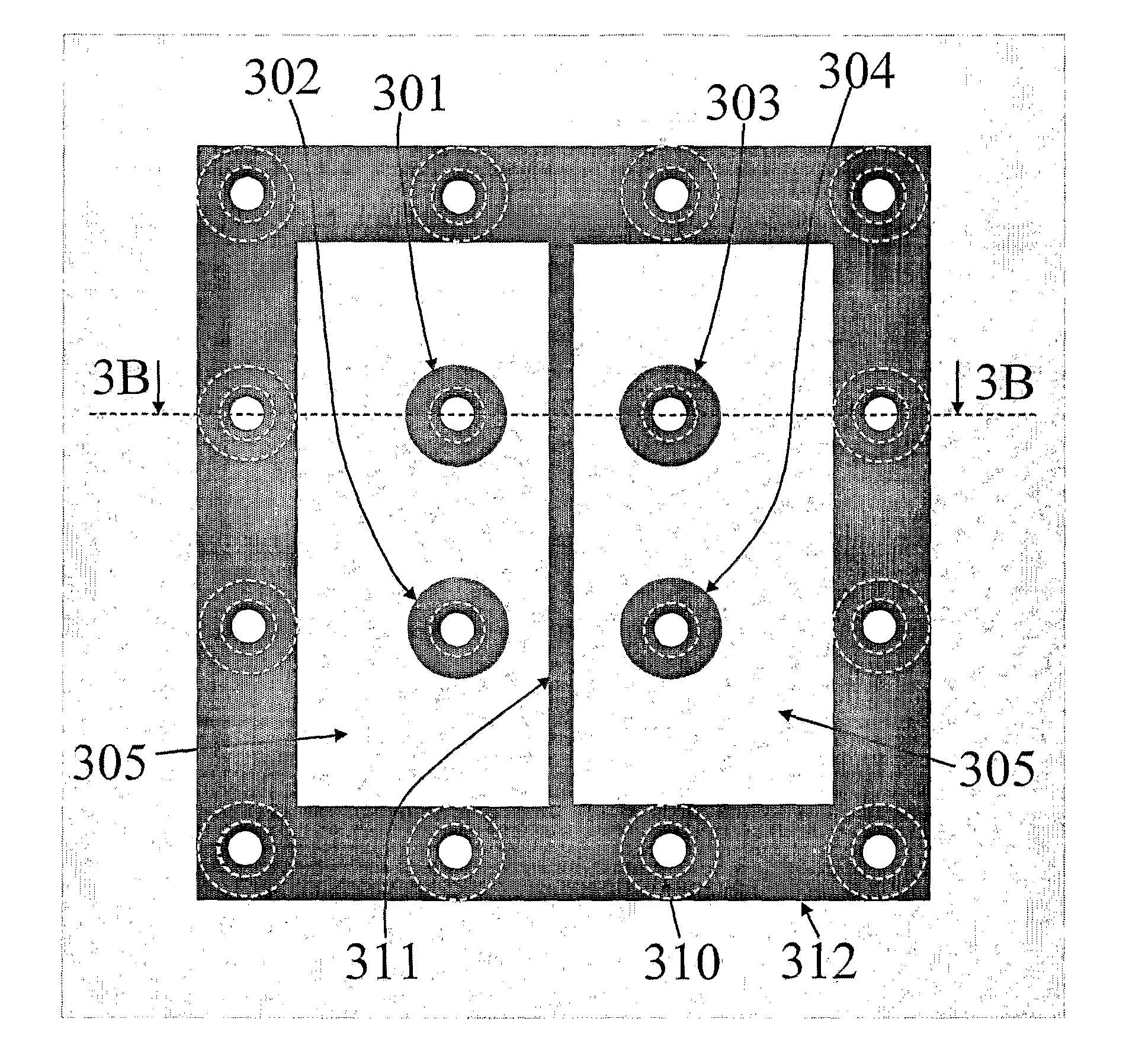
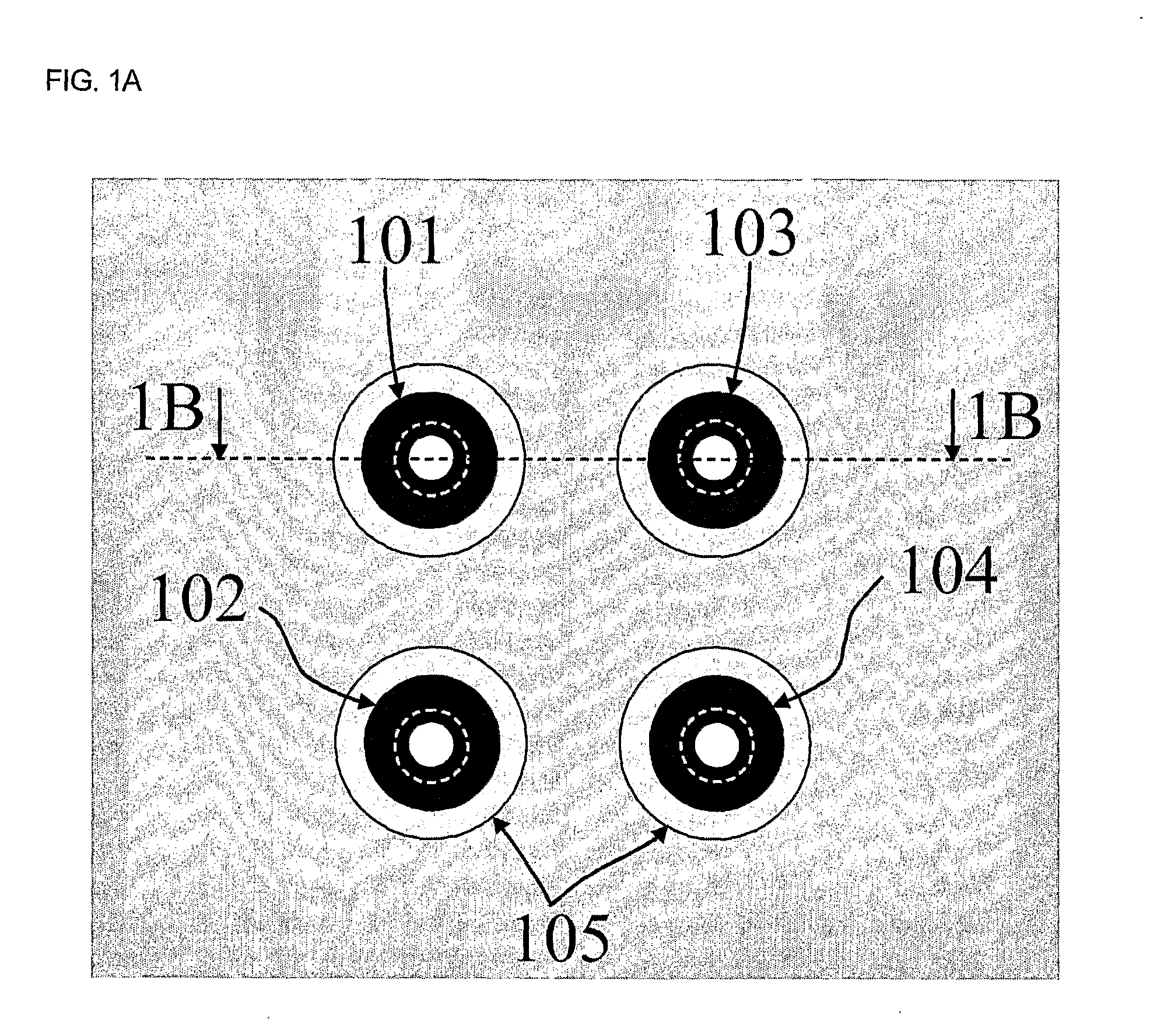
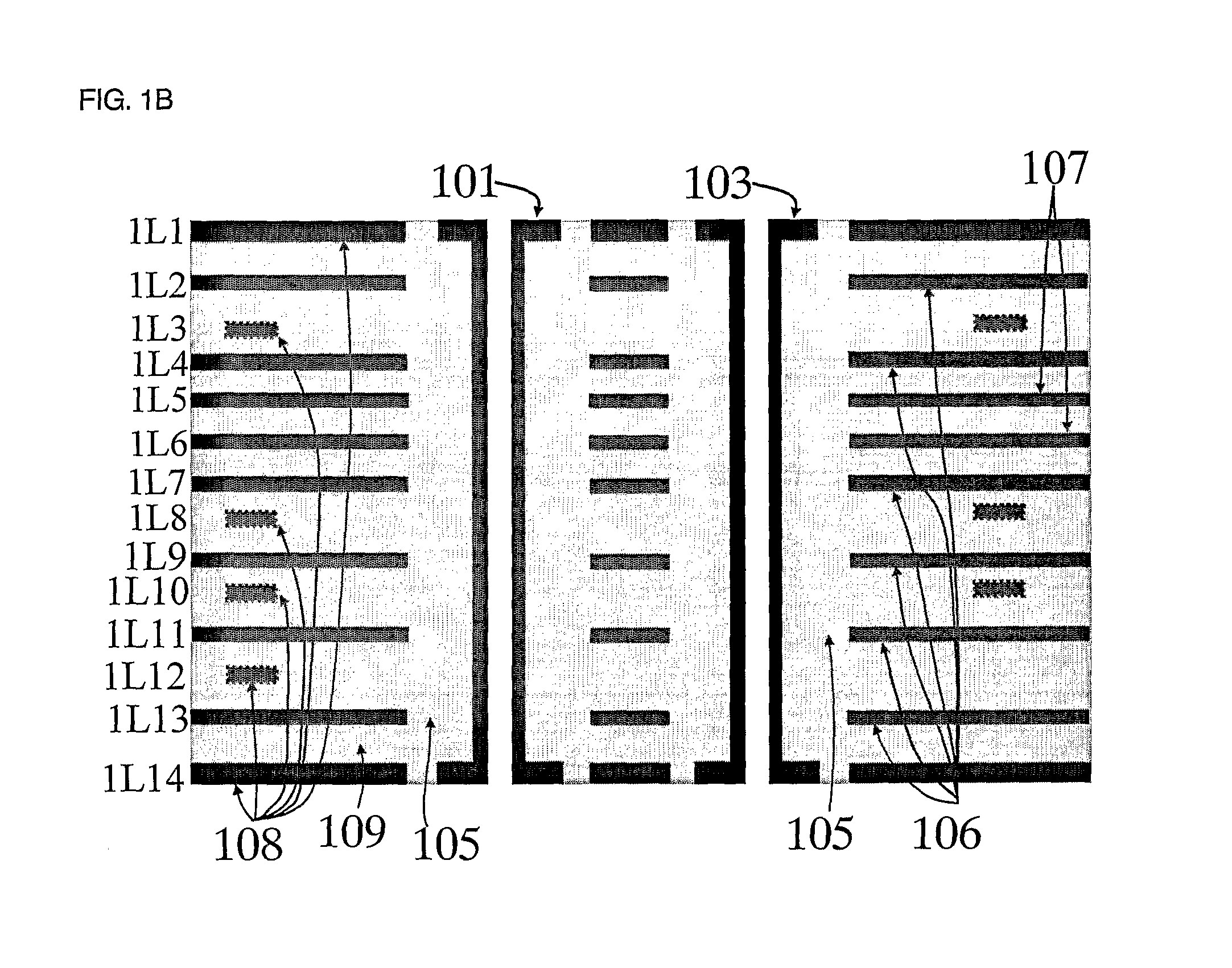
[0078]The first point is the ground shielding around the two signal via pairs. This shielding is formed by both ground vias and ground strips connected with each other at the conductor layers of the multilayer substrate.

[0079]The second point is a method according to which a minimal skew in the via pair is provided for differential signaling. In the method, it can be achieved by an appropriate arrangement of ground vias, corresponding width of the ground strip and symmetrical position of signal via pairs relatively to the ground shield...


PUM


Abstract

To provide more compact dimensions of a via structure formed by signal via pairs and ground vias in multilayer substrate. A multilayer substrate is provided such that the multilayer substrate comprising a high-isolated via cell wherein the high-isolated via cell comprises: two signal via pairs; a shield structure around two signal via pairs consisting of ground vias and ground strips connected to ground vias wherein the shield structure is formed symmetrically in respect to two via pairs to reduce the transformation between mixed modes and also leakage from two signal via pairs; a clearance hole separating signal via pairs from other conductive parts of the multilayer substrate and having predetermined dimensions to provide broadband operation of the high-isolated via cell; and the separating strip disposed symmetrically between said signal via pairs to provide crosstalk reduction between two signal via pairs and common mode decrease.

Description

[0001]This application is based upon and claims the benefit of priority from Japanese patent application No. 2006-280458, filed on Oct. 13, 2006, the disclosure of which is incorporated herein in its entirety by reference.TECHNICAL FIELD[0002]The present invention relates to a multilayer substrate used for differential signaling in which vertical transitions between planar conductor layers of the substrate are formed as a high-isolated cell consisting of two signal via pairs, a shielding structure around the signal via pairs, clearance hole separating the signal via pairs from other conductive parts of the multilayer substrate, strip segment between signal via pairs serving for the reduction of the crosstalk effects between the signal via pairs and common mode suppression in the area of the vertical transitions.[0003]Also, this invention gives structures for the crosstalk effect reduction by means of both the use of ground via shield around the signal via pairs and an appropriate ar...

Claims


Application Information

Patent Timeline
Patent Type & Authority Applications(United States)
IPC IPC(8): H05K9/00H05K1/11G06F17/50
CPCH05K1/0237H05K3/429H05K2201/09236H05K1/0219H05K2201/09636H05K2201/09718H05K2201/09618
Inventor KUSHTA, TARAS
Owner NEC CORP
Why Eureka
Try Eureka