Polishing method

a technology of polishing method and glass, which is applied in the direction of photomechanical equipment, lapping machines, instruments, etc., can solve the problems of increasing the time required for mask blank production, reducing the polishing rate, and generating scratches on the surface of glass substrate, so as to prolong the time necessary for polishing and suppress the generation of scratches

Inactive Publication Date: 2011-08-25
TOKYO ELECTRON LTD
View PDF3 Cites 12 Cited by
  • Summary
  • Abstract
  • Description
  • Claims
  • Application Information

AI Technical Summary

Benefits of technology

The CMP is performed by using a polishing liquid (referred to as a slurry in the art) that contains abrasive particles for polishing a glass substrate. One factor associated with defects found on the surface of a glass substrate is that the abrasive particles contained in the slurry cause scratches on the surface of the glass substrate during polishing. As an approach of suppressing the generation of the scratches, it may be considered to reduce the particle diameters of the abrasive particles. However, this approach is problematic in that the polishing rate decreases and the time necessary to manufacture mask blanks increases.
Thus, in light of the foregoing, it is an object of some embodiments disclosed herein to provide a polishing method of performing appropriate pre-treatments to glass to suppress the generation of the scratches as well as the prolongation in the time necessary for polishing.

Problems solved by technology

One factor associated with defects found on the surface of a glass substrate is that the abrasive particles contained in the slurry cause scratches on the surface of the glass substrate during polishing.
However, this approach is problematic in that the polishing rate decreases and the time necessary to manufacture mask blanks increases.

Method used


Image

  • Polishing method
  • Polishing method
  • Polishing method

Examples


Embodiment Construction

Embodiments will now be described in detail with reference to the accompanying drawings.

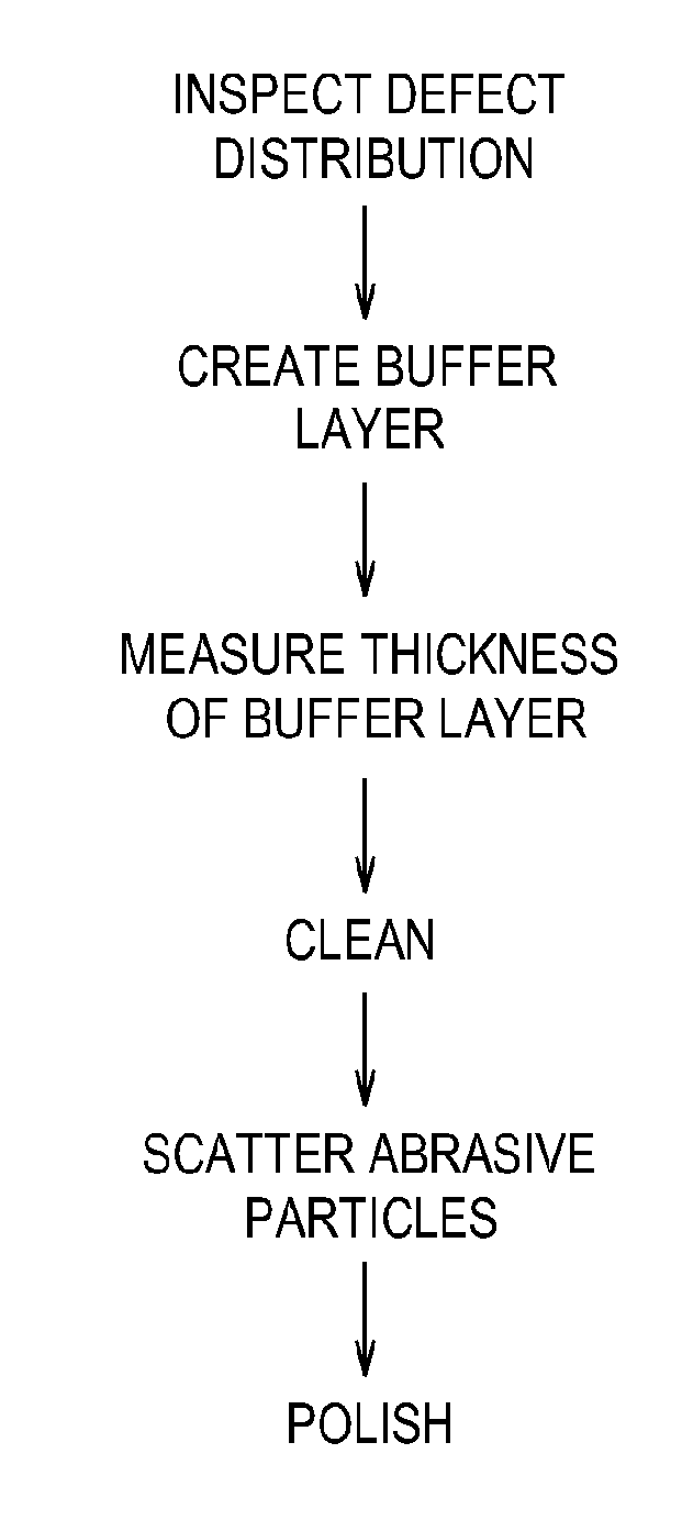
FIG. 1 is a conceptual diagram showing example processes of a polishing method. First, a defect distribution in the vicinity of a surface of a polishing target object (glass substrate) is inspected by a positron annihilation gamma ray measurement. Next, a buffer layer that is easier to polish than glass is created on the surface of the glass substrate. Thereafter, a thickness of the created buffer layer is measured by a positron annihilation gamma ray measurement. Next, the surface of the glass substrate is cleaned. Further, abrasive particles for a slurry are scattered and a liquid component for the slurry is added. Thereafter, the glass substrate is polished from the buffer layer by CMP (Chemical Mechanical Polishing). Hereinafter, detailed descriptions will be provided on each process of the polishing method.

A process of inspecting a defect distribution in the vicinity of the surface of the gl...


PUM

PropertyMeasurementUnit
particle diameteraaaaaaaaaa
brittleaaaaaaaaaa

Abstract

A defect distribution in the vicinity of a surface of a glass substrate is inspected by a positron annihilation gamma ray measurement. A buffer layer including a brittle layer and / or a coating layer is created on the surface of the glass substrate. The brittle layer is formed by irradiating a gas cluster ion on the surface to deteriorate the glass. The coating layer is formed by coating the surface with a soft substance. Next, a thickness of the created buffer layer is measured by a positron annihilation gamma ray measurement. The surface of the glass substrate is then cleaned. To create a slurry, abrasive particles for the slurry are uniformly scattered on a polishing implement for polishing the glass substrate and a liquid component for the slurry is added thereto. The glass substrate is then chemically mechanically polished from the buffer layer with the slurry.

Description

CROSS-REFERENCE TO RELATED APPLICATIONSThis application is based upon and claims the benefit of priority from Japanese Patent Application No. 2010-037398, filed on Feb. 23, 2010, the entire contents of which are incorporated herein by reference.TECHNICAL FIELDThe present disclosure relates to a method of polishing glass using chemical mechanical polishing.BACKGROUNDCircuit patterns on electronic components such as a semiconductor element are made by using an exposure technology, for example, by reductively projecting a negative circuit pattern formed on a photo mask to a silicon wafer. To promote miniaturization of electronic components, the wavelength of light used in exposure technology becomes shorter and shorter. Recently, an EUV exposure technology using an EUV (Extreme Ultraviolet) light as the exposure light has been developed. A photo mask for the EUV exposure is structured such that a multi-layered film including metal and a semiconductor for reflecting EUV light is provide...

Claims


Application Information

Patent Timeline
Patent Type & Authority Applications(United States)
IPC IPC(8): C03C15/00B24B7/24B24B37/00B24B49/10C03C19/00
CPCB24B37/005B24B37/042C03C23/0005C03C19/00C03C17/28G03F7/2041G03F7/7065H01L21/0274
Inventor MORIYA, TSUYOSHI
Owner TOKYO ELECTRON LTD
Why Eureka
Try Eureka