hBN INSULATOR LAYERS AND ASSOCIATED METHODS

Inactive Publication Date: 2011-08-25
SUNG CHIEN MIN +4
View PDF15 Cites 26 Cited by
  • Summary
  • Abstract
  • Description
  • Claims
  • Application Information

AI Technical Summary

Benefits of technology

[0011]In another aspect of the present invention, a light-emitting diode device having improved heat dissipation properties is provided having a light-emitting diode thermally coupled to a printed circuit board according to aspects of the present invention, such that the electrically insulating layer is operable to accelerate heat movement away from the light-emitting diode.
[0012]In yet a

Problems solved by technology

As electronic circuitry increases in speed and decreases in size, cooling of such devices becomes problematic.
As it builds, heat can cause various thermal problems associated with both the printed circuit board and internally in many electronic components.
Significant amounts of heat can affect the reliability of an electronic device, or even cause it to fail by, for example, causing burn out or shorting both within the electronic components themselves and across the surface of the printed circuit board.
Thus, the buildup of heat can ultimately affect the f

Method used


Image

  • hBN INSULATOR LAYERS AND ASSOCIATED METHODS
  • hBN INSULATOR LAYERS AND ASSOCIATED METHODS

Examples


example

Example 1

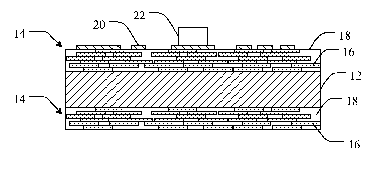
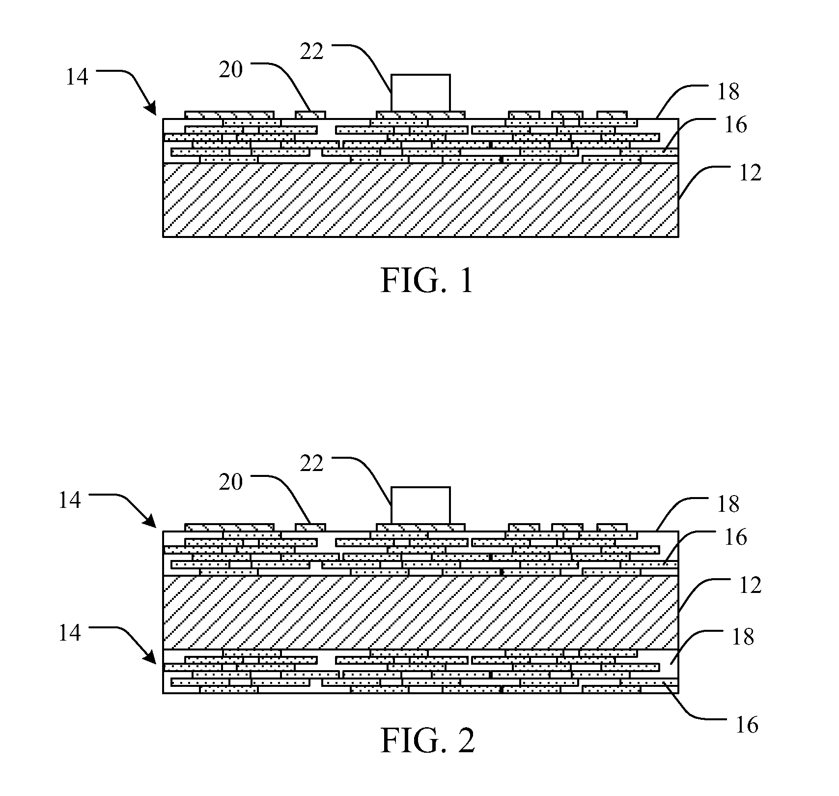
[0062]hBN is mixed with an organic binder that is dissolved in an organic solvent. The slurry is spray coated onto an aluminum substrate cured to remove solvent. The resulting layer is an approximately 50 micron thick insulating layer that can spread heat. This electrically insulating layer is sputtered with Cr and electroplated with Cu. The Cu is then etched to form circuit elements. An LED chip is then mounted on the substrate and electrically coupled to the circuit elements. The LED chip is cooled by the electrically insulating layer that conducts heat to the aluminum substrate.

example 2

[0063]hBN is mixed with SnO2 nanopowder and then plasma sprayed onto an aluminum substrate. The hBN / SnO2 layer has improved thermal conductivity as it does not contain an organic binder. This electrically insulating layer is then sputtered with Cr and electroplated with Cu, and the Cu is etched to form circuit elements.

example 3

[0064]A 24 inch (610 mm)×18 inch (457 mm) Metal Core Printed Circuit Board (MCPCB) is made by laminating a 70 micron thick epoxy resin on a 2 mm thick aluminum substrate (1050, 5052 or 6061) and 50 micron thick copper foil. The epoxy resin is premixed with 65 wt % of solid content which contains 80:20 of Al2O3 (1-2 micron grain size) and hBN powder so that the weight of the hBN accounts for 13% of the total weight. The MCPCB is then tested for peel strength and thermal conductivity. When the hBN particle size is 10 microns, K value is 4 W / mk and the peeling strength is 6 lbs / in2. When the hBN particle size is 2 microns, the k value is 3.5 W / mK and the peeling strength is 9 lbs / in2. When a mixture of hBN sizes is used (2 microns and 10 microns at 3:1), the K value is 4.5 W / mk and the peeling strength is 8 lbs / in2.


PUM

PropertyMeasurementUnit
Particle sizeaaaaaaaaaa

Abstract

Electrically insulating layers having increased thermal conductivity, as well as associated devices and methods are disclosed. In one aspect, for example, a printed circuit board is provided including a substrate and an electrically insulating layer coated on at least one surface of the substrate, the electrically insulating layer including a plurality of hBN particles bound in a binder material.

Description

PRIORITY DATA[0001]This application claims the benefit of U.S. Provisional Patent Application Ser. No. 61 / 298,458, filed on Jan. 26, 2010, which is incorporated herein by reference in its entirety. This application also claims benefit of Chinese Patent Application Serial no. 201010167406.0, filed on Apr. 27, 2010.FIELD OF THE INVENTION[0002]The present invention relates generally to hexagonal boron nitride materials in electronic applications. Accordingly, the present invention involves the electrical and material science fields.BACKGROUND OF THE INVENTION[0003]In many countries, major portions of the populations consider electronic devices to be integral to their lives. Such increasing use and dependence has generated a demand for electronics devices that are smaller and faster. As electronic circuitry increases in speed and decreases in size, cooling of such devices becomes problematic.[0004]Electronic devices generally contain printed circuit boards having integrally connected el...

Claims


Application Information

Patent Timeline
IPC IPC(8): H01L33/64C09K5/08H05K1/00H05K1/03H05K7/20F28F7/00
CPCH05K1/0366H05K1/0373H05K1/056Y10T428/24893H05K2201/10106H05K1/0203Y10T428/2481H05K2201/0209
Inventor SUNG, CHIEN-MINHU, SHAO CHUNGTENG, CHIEN-CHUNGYANG, SHANG-RAYSUNG, MICHAEL
Owner SUNG CHIEN MIN
Why Eureka
Try Eureka