Solid-state image pickup deviceand fabrication process thereof

Inactive Publication Date: 2011-08-25
SONY CORP
View PDF3 Cites 21 Cited by
  • Summary
  • Abstract
  • Description
  • Claims
  • Application Information

AI Technical Summary

Benefits of technology

[0042]In the solid-state image pickup device according to the embodiment of the present invention, the impurity concentration distribution in the proximity of the boundary between the P-type region and the N-type region becomes an impurity concentration distribution having a so-called steep concentration gradient. It is, therefore, possible to increase the saturation charge quantity Qs.
[0043

Problems solved by technology

It is, therefore, difficult to form a steep impurity concentration profile.
Moreover, such deviations from individual device parameters cause deteriorations of the sensor characteristics, the occurrence

Method used


Image

  • Solid-state image pickup deviceand fabrication process thereof
  • Solid-state image pickup deviceand fabrication process thereof
  • Solid-state image pickup deviceand fabrication process thereof

Examples


first embodiment

1. First Embodiment

[First Example of the Configuration of Solid-State Image Pickup Device]

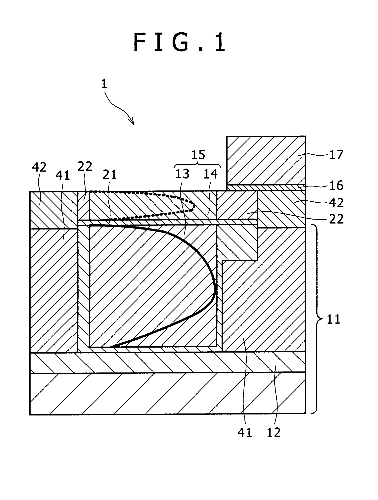
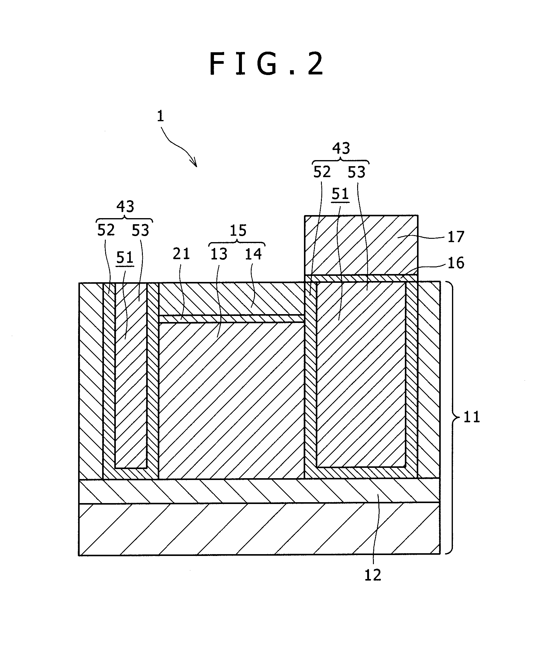
[0078]The first example of the configuration of the solid-state image pickup device according to the first embodiment of the present invention will be described with reference to the schematic sectional configuration view shown in FIG. 1.

[0079]As shown in FIG. 1, a silicon substrate is used as a semiconductor substrate 11, and a P-type buried region 12 doped with boron (B) is formed in the semiconductor substrate 11. This P-type buried region 12 serves as an overflow barrier region for a light-receiving sensor section (photodiode) of the HAD structure.

[0080]On the semiconductor substrate 11 above the P-type buried region 12, inter-pixel isolation regions 41 are formed to isolate pixels. These inter-pixel isolation regions 41 are formed, for example, of P-type impurity regions. These P-type impurity regions are formed, for example, of boron-doped regions.

[0081]On the semiconductor substrate 11, ...

second embodiment

2. Second Embodiment

[First Example of Fabrication Process of Solid-State Image Pickup Device]

[0111]The first example of the fabrication process of the solid-state image pickup device according to the second embodiment of the present invention will be described with reference to the schematic sectional fabrication-process views shown in FIGS. 3A through 3G. The description will be made taking a CMOS image sensor as an example. It is to be noted that concerning a removal step of a resist film and a formation step of a logic section, a description is omitted herein unless otherwise specifically indicated.

[0112]As illustrated in FIG. 3A, a silicon substrate is provided as a semiconductor substrate 11.

[0113]On the semiconductor substrate 11, an oxide film 31 is next formed to serve as a buffer film upon ion implantation. This oxide film 31 may be formed, for example, with a silicon oxide film, for example, by a thermal oxidation method, a chemical vapor growth method, or the like.

[0114]O...

third embodiment

3. Third Embodiment

[A] Device Configuration, Etc.

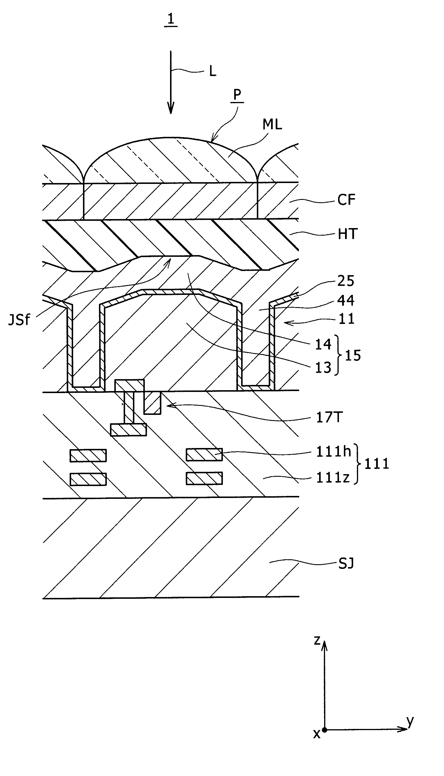
[0223]FIGS. 14 and 15 are views illustrating certain essential parts of the solid-state image pickup device 1 according to the third embodiment of the present invention. In FIG. 14, a section of a pixel P is illustrated. On the other hand, FIG. 15 illustrates a circuit configuration of the pixel P.

[0224]As illustrated in FIGS. 14 and 15, this embodiment is different in some configuration from the first embodiment, but includes certain common parts. With respect to these common parts, a description is thus omitted wherever appropriate.

[0225]As illustrated in FIGS. 14 and 15, the solid-state image pickup device 1 has pixels P. These pixels P are arranged such that in a plane (x-y plane) of a semiconductor substrate 11, plural ones of them are arrayed in each of a horizontal direction x and a vertical direction y extending at right angles relative to the horizontal direction x.

[0226]Each pixel P includes a photodiode 15 and a pixel trans...


PUM


Abstract

A solid-state image pickup device has photodiodes, each of which includes an N-type region formed in a semiconductor substrate, a first silicon carbide layer formed above the N-type region, and a P-type region including a first silicon layer formed above the first silicon carbide layer and doped with boron. A fabrication process of such a solid-state image pickup device is also disclosed.

Description

[0001]The present application claims priority to Japanese Patent Applications JP 2010-127690 and 2009-202301 filed in the Japanese Patent Office on Jun. 3, 2010 and Sep. 2, 2009, respectively, the entire contents of which is hereby incorporated by reference.BACKGROUND OF THE INVENTION[0002]1. Field of the Invention[0003]This invention relates to a solid-state image pickup device and its fabrication process.[0004]2. Description of the Related Art[0005]For solid-state image pickup devices, it has been common to adopt the front-side illuminated structure that electrodes and wirings are formed over a surface of a substrate, in which photoelectric converting sections are formed, and light is allowed to enter from above the electrodes and wirings. In solid-state image pickup devices such as CCD (Charge Coupled Devices) and CMOS (Complementary Metal Oxide Semiconductor) sensors that make use of silicon substrates as such substrates, a buried structure is adopted in recent years for photoel...

Claims


Application Information

Patent Timeline
IPC IPC(8): H01L27/146H01L31/18
CPCH01L21/02529H01L21/02532H01L27/14687H01L27/1463H01L27/1464H01L21/0262
Inventor OHCHI, TOMOKAZUMIYANAMI, YUKIARAKAWA, SHINICHI
Owner SONY CORP
Why Eureka
Try Eureka