Polymer waveguide fabrication process

a polymer and waveguide technology, applied in the field of polymer waveguide fabrication, can solve the problems of excessive evaporation and removal of these components, and achieve the effects of superior properties and manufacturability, and elimination of residual volatiles

Inactive Publication Date: 2006-03-14
ENABLENCE TECH USA
View PDF7 Cites 23 Cited by
  • Summary
  • Abstract
  • Description
  • Claims
  • Application Information

AI Technical Summary

Benefits of technology

[0016]The present invention provides an improved process for forming polymeric waveguides from photopolymerizable materials. Initially, after a rigorous chemical cleaning of a substrate, the substrate may be primed with acrylate functionalized chloro- or alkoxy-type silane compounds. This is followed by an optional application of a tie layer of a highly crosslinkable acrylate monomer mixture followed by deoxygenation under vacuum, under purging with nitrogen gas, or under a combination of vacuum and purging. Deoxygenation is followed by a blanket UV cure of the film to a level below its full cure. The choice of deoxygenation conditions being either vacuum or purge gas or a combination of these two is driven by material and process considerations. In the case where process time for degassing must be kept to a minimum, vacuum degassing is desired. The low ambient pressure acts as a physical force to speed emission of dissolved gases. However, if components in the photopolymerizable material are easily evaporated, then extensive vacuum degassing can cause excessive evaporation and removal of these components, which is typically not desirable. Purging with nitrogen gas would be done in this case. Next follows an application of a layer of buffer material having a refractive index of about 1% to about 3% less than that of the core, also followed by deoxygenation under vacuum, under purging with nitrogen gas, or under a combination of vacuum and purging. Deoxygenation is followed by a blanket UV cure of the film to a level below its full cure. Thereafter, a layer of clad material having a refractive index of about 0.3% to about 1.5% less than that of the core is optionally applied and followed by deoxygenation under vacuum, under purging with nitrogen gas, or under a combination of vacuum and purging. Deoxygenation is again followed by a blanket UV cure of the film to a level below its full cure. Next the layer of core material is applied. After the core material is applied, a photomask is lowered to a predetermined level above the core layer. Usually the mask is 500 or more μm away during the deoxygenation stage and is typically lowered to from about 0 μm to about 20 μm above the core layer, and more usually from about 5 μm to about 20 μm above the core layer. After the core layer material and mask are in place, deoxygenation under vacuum, under purging with nitrogen gas, or under a combination of vacuum and purging, is followed by UV cure of the waveguide pattern to a level below the full cure of the waveguide cores. The non-exposed core material may then be developed with a fluorinated solvent, followed by application of an overclad layer of clad material and then by deoxygenation under vacuum, under purging with nitrogen gas, or under a combination of vacuum and purging. Deoxygenation is followed by a blanket UV cure of the film to a fully cured level. Finally, the overall composition may be thermally annealed to fully cure the buffer composition, clad composition and core composition and eliminate any residual volatiles. This process having extensive and controlled deoxygenation via vacuum and purging with nitrogen gas produces intermediate stage layers of photopolymerizable material having very low quantities of dissolved and gaseous oxygen, resulting in production of waveguides having superior properties and manufacturability.

Problems solved by technology

However, if components in the photopolymerizable material are easily evaporated, then extensive vacuum degassing can cause excessive evaporation and removal of these components, which is typically not desirable.

Method used


Image

  • Polymer waveguide fabrication process
  • Polymer waveguide fabrication process
  • Polymer waveguide fabrication process

Examples


example 1

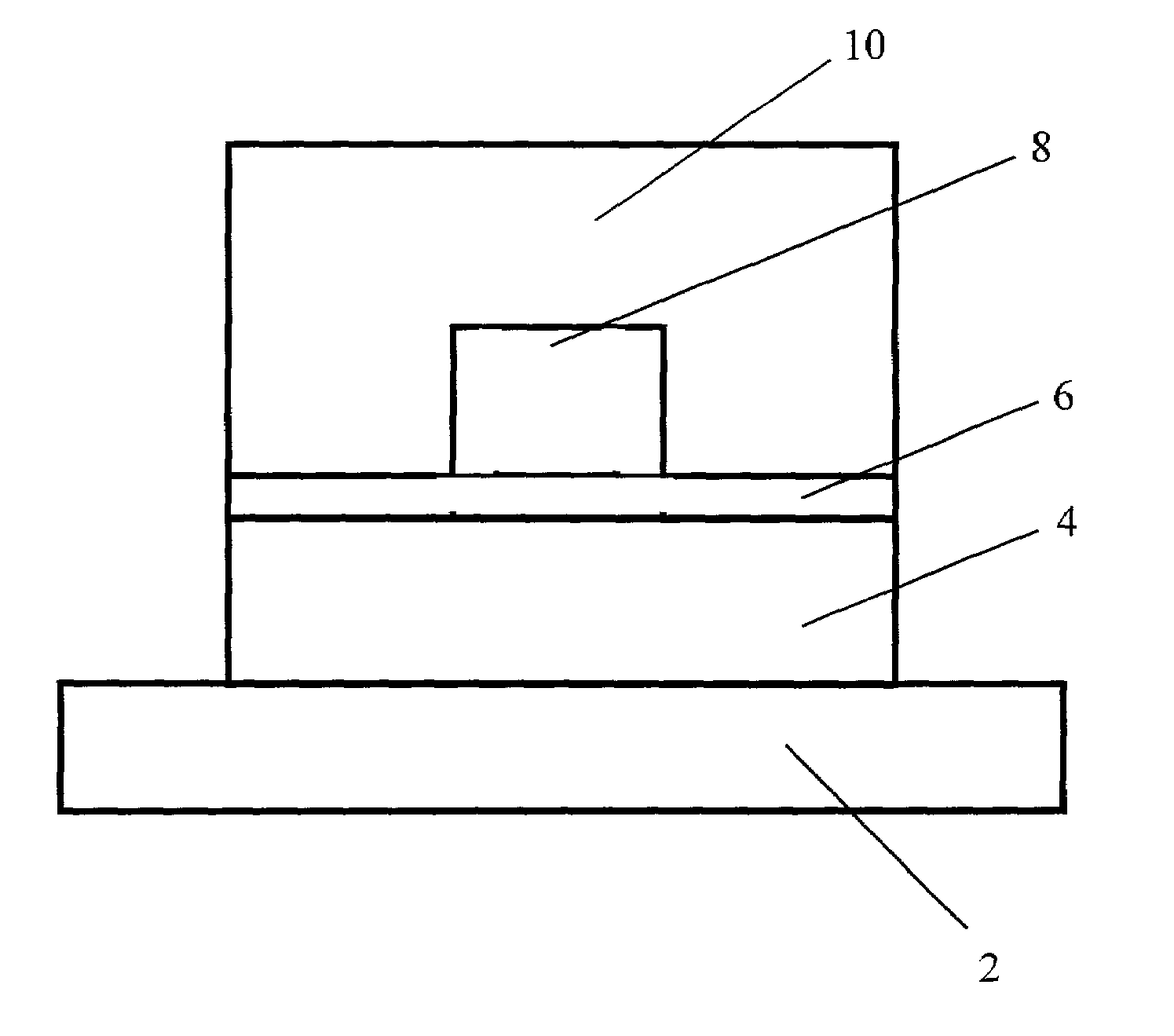
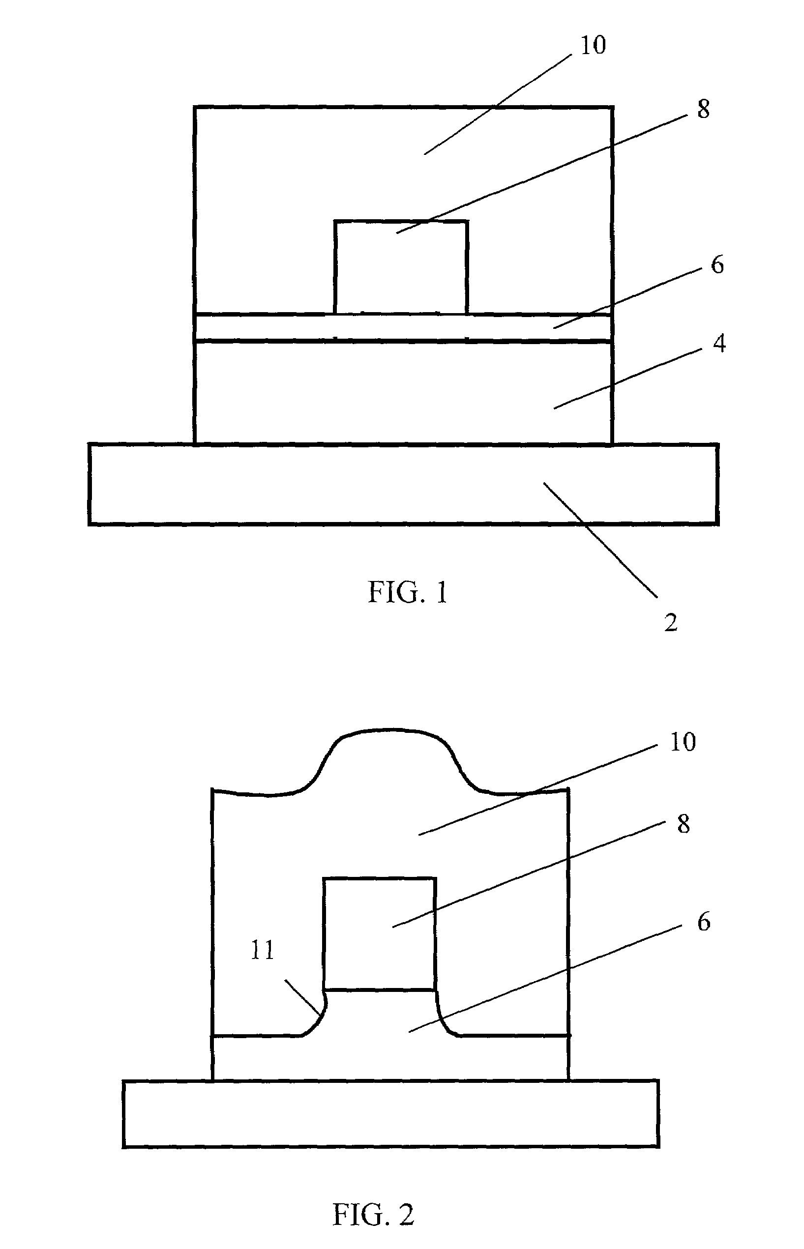
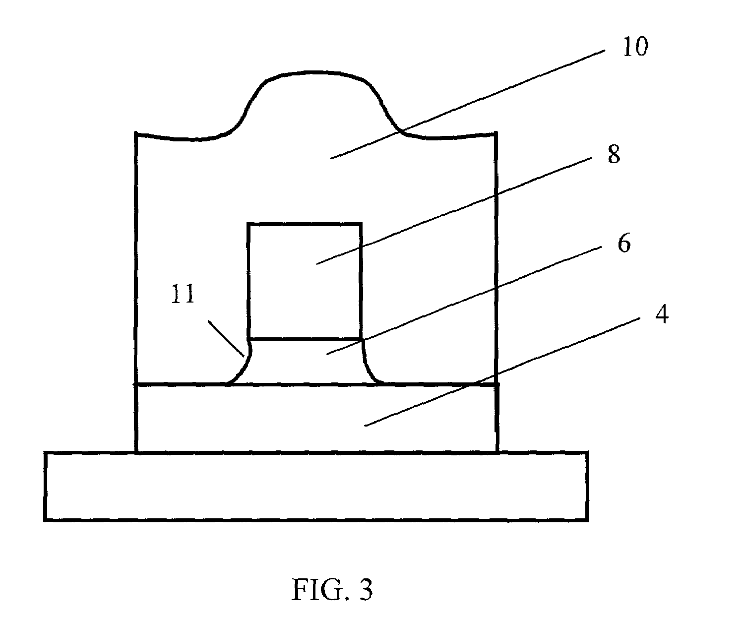
[0062]The process described herein was applied to the production of an array of planar polymer waveguides on a silicon wafer. This process was demonstrated to have advantages in ease of use and ease of scalability. Additionally, the process produced fabricated waveguides with high uniformity of such physical features as layer thickness and waveguide geometry, and with very low optical insertion loss at important telecommunication waveguides of roughly 1.3 μm and 1.55 μm.

[0063]A 100-mm diameter 4″ silicon wafer with a 500 nm thick oxide layer was obtained in a clean state from the wafer manufacturer. The silicon substrate was treated by soaking in 4 M NaOH solution for 1 hour, followed by rinsing under flowing de-ionized water for 15 minutes. The NaOH treatment is meant to ensure complete functionalization of the silicon oxide surface with OH groups. The silicon wafer was dried by blowing off excess water and baking on a 120° C. hot plate for 10 minutes. Neat (3-acryloxypropyl)trichl...


PUM


Abstract

The invention relates to a process a process for forming single-mode, organic waveguides employing organic polymeric materials. The process reduces dissolved and gaseous oxygen content to very low quantities, resulting in production of waveguides having superior properties and manufacturability. Also provided is a process for preventing loss of light due to cores having flared ends. A waveguide is produced by sequentially a layer of a liquid, photosensitive buffer and clad composition to a surface of a substrate; deoxygenating under vacuum; overall exposing under an inert gas actinic radiation to partially polymerize the compositions below a full curing. Coating a photosensitive core composition to the clad composition; deoxygenating under vacuum, covering with an inert gas atmosphere; positioning a photomask above, but not in contact with the core layer; imagewise exposing the core through a photomask pattern to actinic radiation to partially polymerize the core composition; developing core; coating a photosensitive overclad composition over the image areas of the core composition; deoxygenating under vacuum; overall exposing the overclad composition, under inert gas to actinic radiation to substantially fully cure the optional buffer composition, the underclad composition, the core composition and the clad composition.

Description

BACKGROUND OF THE INVENTION[0001]1. Field of the Invention[0002]The present invention relates to the formation of polymeric optical waveguides, or more particularly to a process for forming single-mode, organic waveguides employing organic polymeric materials. The process reduces dissolved and gaseous oxygen content to very low quantities, resulting in production of waveguides having superior properties and manufacturability.[0003]2. Technical Background[0004]In optical communication systems, messages are transmitted by carrier waves at optical frequencies that are generated by such sources as lasers and light-emitting diodes. There is interest in such optical communication systems because they offer several advantages over conventional communication systems. They have a greatly increased number of channels of communication as well as the ability to transmit messages at much higher speeds than electronic systems using copper wires. This invention is concerned with the formation of l...

Claims


Application Information

Patent Timeline
Patent Type & Authority Patents(United States)
IPC IPC(8): G02B6/10G02B6/122G02B6/13
CPCG02B6/13G02B6/1221G02B6/02
Inventor FERM, PAUL M.BATTELL, KEVINBEESON, KARL W.MAXFIELD, MACRAEPANT, DEEPTISHACKLETTE, LAWRENCE W.
Owner ENABLENCE TECH USA
Why Eureka
Try Eureka