

High temperature atomic layer deposition of dielectric oxides
a dielectric oxide and atomic layer technology, applied in chemical vapor deposition coatings, electrical devices, coatings, etc., can solve the problems of more or less self-saturation reactions, achieve efficient deposition of thin dielectric oxide layers, reduce capacitors and electronic devices, and improve the effect of technology
- Summary
- Abstract
- Description
- Claims
- Application Information
AI Technical Summary
Benefits of technology
Problems solved by technology
Method used
Image

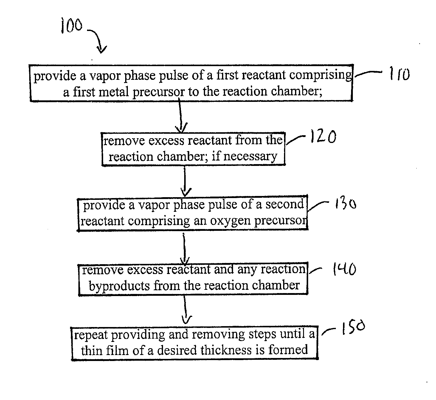
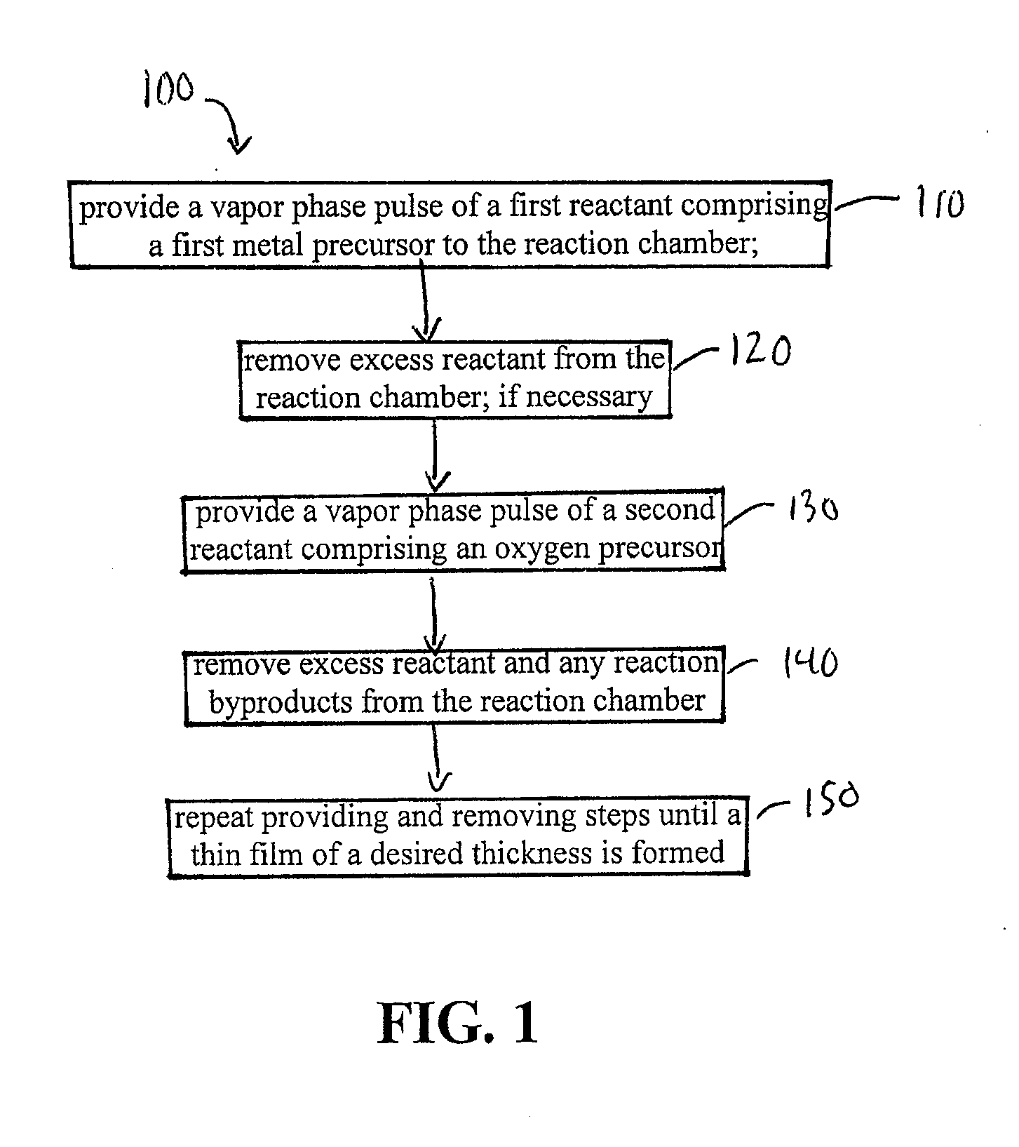
Examples
example 1
[0103]Crystalline layers of TiO2 are deposited by ALD using alternating pulses of TiCl4 and an oxygen source, such as H2 / CO2 with a substrate temperature of above 650° C. Other oxygen sources include O2, O2 / H2, H2 / CO2, H2O, O3, NO, NO2, N2O, and H2O2. The crystallinity of the titanium oxide is typically anatase. The resulting anatase titanium oxide thin film can have an optical transmittance greater than about 60% in the visible spectrum.
example 2
[0104]Crystalline layers of Al2O3 are deposited by ALD from alternating pulses of AlCl3 and an oxygen source, such as H2 / CO2 with a substrate temperatures of above 650° C. Other oxygen sources that can be used include O2, O2 / H2, H2 / CO2, H2O, O3, NO, NO2, N2O, and H2O2. The crystallinity of the aluminum oxide as deposited can be alpha-aluminum oxide.
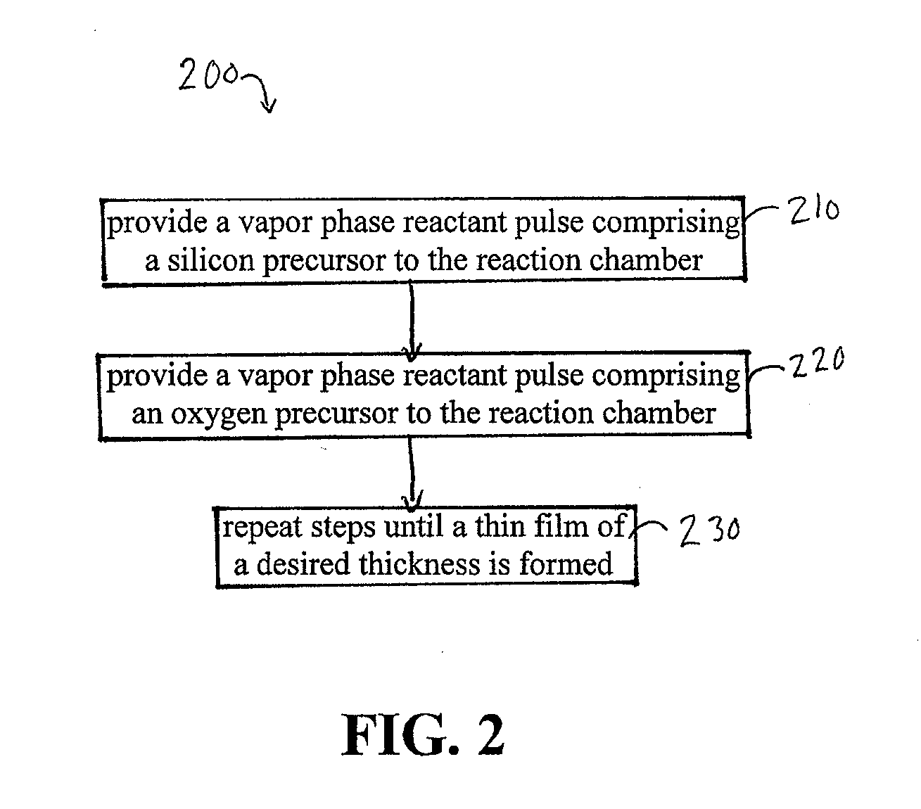
example 3
[0105]SiO2 is deposited by ALD from alternating pulses of SiCl4 and an oxygen source, such as such as H2 / CO2 with a substrate temperature of above 650° C. Other oxygen sources include O2, O2 / H2, H2 / CO2, H2O, O3, NO, NO2, N2O, and H2O2. The crystallinity of the silicon dioxide can be quartz, for example alpha or beta quartz. At lower deposition temperatures amorphous silicon dioxide is deposited. Silicon dioxide can also be deposited using SiF4.
PUM
| Property | Measurement | Unit |
|---|---|---|
| Temperature | aaaaa | aaaaa |
| Temperature | aaaaa | aaaaa |
| Temperature | aaaaa | aaaaa |
Abstract
Description
Claims
Application Information