Pattern transfer method and apparatus, flexible display panel, flexible solar cell, electronic book, thin film transistor, electromagnetic-shielding sheet, and flexible printed circuit board applying thereof

Inactive Publication Date: 2011-09-01
KOREA ADVANCED INST OF SCI & TECH
View PDF13 Cites 31 Cited by
  • Summary
  • Abstract
  • Description
  • Claims
  • Application Information

AI Technical Summary

Benefits of technology

[0067]According to the present invention, it may further provide a pattern transfer method capable of rapidly manufacturing a pattern at a low cost.
[0068]According to the present invention, it may further provide a pattern transfer method in which a substrate on which a pattern is transferred is not transformed by heat.
[0069]According to the present invention, it may further provide a pattern transfer method in which patterning is possible in a substrate having low thermal resistan

Problems solved by technology

However, the conventional manufacturing methods have their own limitations in the process respectively.
First, in the photolithography, a manufacturing process is complicated, it is difficult to manufacture a shadow mask, a manufacturing cost is high, and precision is deteriorated due to distortion of a mask.
Furthermore, it is difficult to align the mask and a target, and to change a process, namely, to change the size and the shape of a pattern.
Second, the FMD has the same problems associated with the shadow mask described in the photolithography and a problem that a manufacturing cost is high.
Furthermore, the FMD has problems such as material limitation and long manufacturing time.
Third, because the material manufacturing a pattern should be a liquid solution state in an ink-jet type in the printing, various materials cannot be used.
Because it is difficult to inject a solution uniformly, a non-uniform pattern is produced.
Further, when a substrate having a pattern to be transferred is a flexible substrate, because the flexible substrate is decomposed by heat at the time of ink sintering, sintering temperature is restricted.
Accordingly, an ink-jet type is not suitable to be used in a substrate such as PET having low thermal resistance.
However, since a roll type mold has a pattern of a geometric shape, it is difficult to manufacture the mold.
Fifth, since the NIL scheme performs patterning through etching using photoresist (PR), it is not a direct patterning scheme and a PR remains to complicate a procedure for manufacturing a pattern and surface treatment is required to easily space a mold.
Furthermore, it is difficult

Method used


Image

  • Pattern transfer method and apparatus, flexible display panel, flexible solar cell, electronic book, thin film transistor, electromagnetic-shielding sheet, and flexible printed circuit board applying thereof
  • Pattern transfer method and apparatus, flexible display panel, flexible solar cell, electronic book, thin film transistor, electromagnetic-shielding sheet, and flexible printed circuit board applying thereof
  • Pattern transfer method and apparatus, flexible display panel, flexible solar cell, electronic book, thin film transistor, electromagnetic-shielding sheet, and flexible printed circuit board applying thereof

Examples


first embodiment

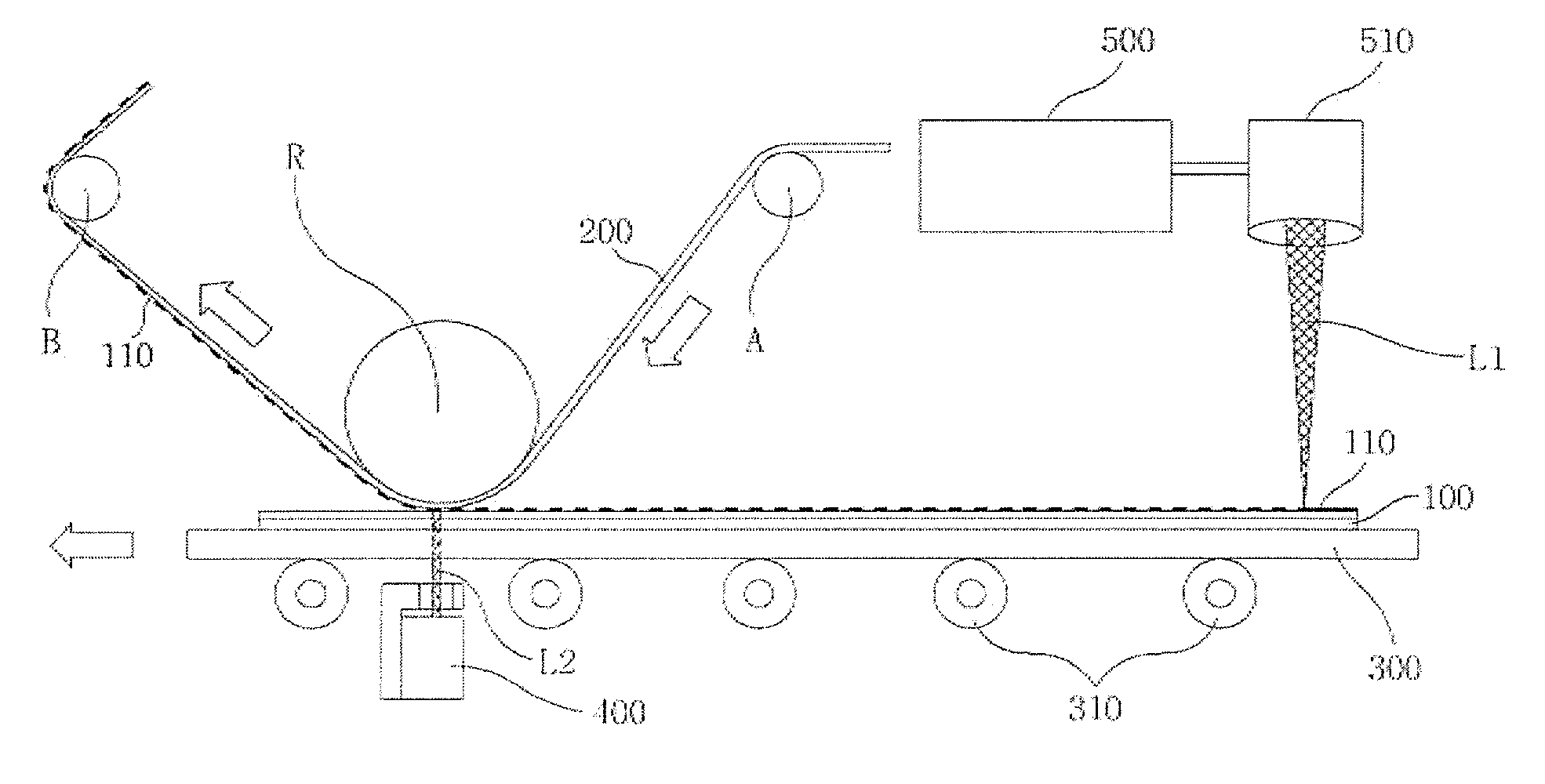
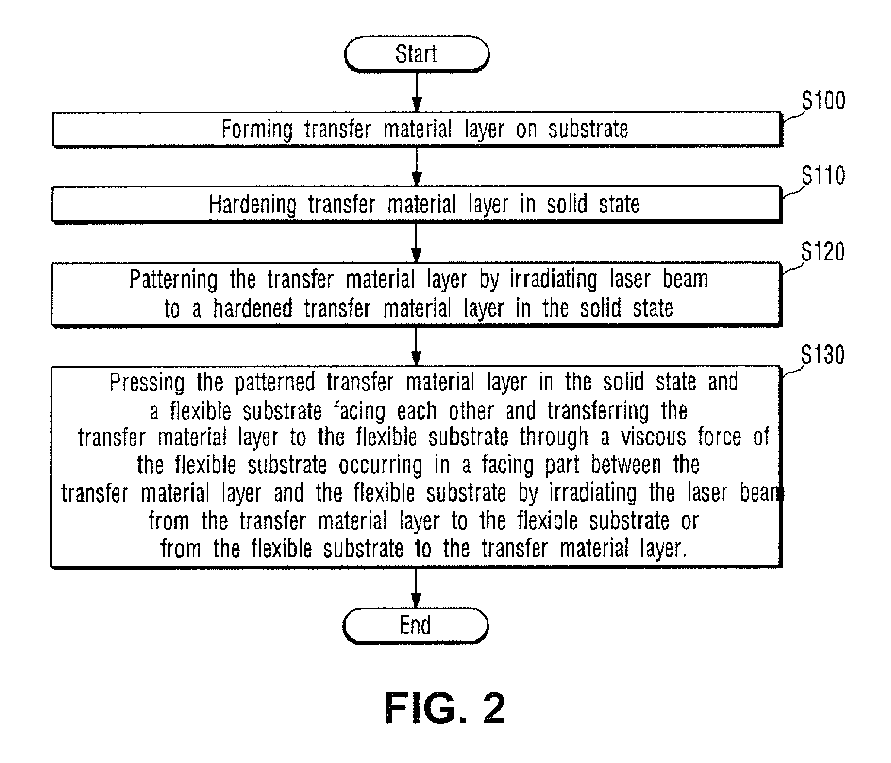
[0091]Referring to FIG. 2, a pattern transfer method according to the present invention comprises: a first step of forming a transfer material layer on a substrate 100 (S100); a second step of hardening the transfer material layer in the solid state (S110); a third step of patterning the transfer material layer by irradiating a laser beam to the hardened transfer material layer in the solid state (S120); and a fourth step of pressing the patterned transfer material layer in the solid state and a flexible substrate 200 facing each other and transferring the transfer material layer to the flexible substrate 200 by a viscous force of the flexible substrate 200 occurring in a facing part between the transfer material layer and the flexible substrate 200 by irradiating the laser beam from the transfer material layer to the flexible substrate 200 or from the flexible substrate 200to the transfer material layer (S130).

[0092]The first step (S100) is a step of forming a transfer material lay...

fourth embodiment

[0124]Referring to FIG. 8, a pattern transfer method according to the present invention includes: a first step (S300) of forming a hydrophobic coating layer 10 on a substrate 20 and selectively removing the hydrophobic coating layer 10 using laser application plasma to form a surface mold 90; a second step (S310) of forming a pattern by providing and drying a pattern material 50 on the surface mold 90, and then by sintering the surface mold 90 at a high temperature; a third step (S320) of pressing the surface mold 90 and a target substrate 80 facing each other and transferring the pattern material 50 to the target substrate 80 by a viscous force of the target substrate 80 occurring in a facing part between the pattern material 50 on the surface mold 90 and the target substrate 80 by irradiating the laser beam from the surface mold 90 to the target substrate 80.

[0125]In the first step (S300), a hydrophobic Self-Assembled Monolayers (referred to as ‘SAM’ hereinafter) is coated on a ha...


PUM

PropertyMeasurementUnit
Flexibilityaaaaaaaaaa
Hydrophilicityaaaaaaaaaa
Hydrophobicityaaaaaaaaaa

Abstract

The present invention relates to methods and apparatuses for transferring pattern, a flexible display panel, a flexible solar cell, an electronic book, a thin film transistor, an electromagnetic-shielding sheet, and a flexible printed circuit board applying thereof. A pattern transfer method related to the present invention comprises: a first step of forming a transfer material layer on a substrate; a second step of hardening the transfer material layer in the solid state; a third step of patterning the transfer material layer by irradiating a laser beam to the hardened transfer material layer in the solid state; and a fourth step of pressing the patterned transfer material layer in the solid state and a flexible substrate facing each other and transferring the transfer material layer to the flexible substrate by a viscous force of the flexible substrate occurring in a facing part between the transfer material layer and the flexible substrate by irradiating the laser beam from the transfer material layer to the flexible substrate or from the flexible substrate to the transfer material layer.

Description

CROSS-REFERENCE TO RELATED APPLICATIONS[0001]This U.S. National stage application claims priority under 35 U.S.C. §119(a) to Korean Patent Application No. 10-2010-0001354, filed in the Republic of Korea on Jan. 7, 2010, Korean Patent Application No. 10-2010-0103480, filed in the Republic of Korea on Oct. 22, 2010, and Korean Patent Application No. 10-2010-0103485, filed in the Republic of Korea on Oct. 22, 2010, the entire contents of which are hereby incorporated herein by reference.BACKGROUND OF THE INVENTION[0002]1. Field of the Invention[0003]The present invention relates to pattern transfer methods and apparatuses, a flexible display panel, a flexible solar cell, an electronic book, a thin film transistor, an electromagnetic-shielding sheet, and a flexible printed circuit board applying thereof.[0004]2. Description of the Related Art[0005]Recently, a demand for thin films and high performance of a product has been increasing in a lighting device industry, a display industry, a ...

Claims


Application Information

Patent Timeline
IPC IPC(8): H01L31/0224C23C14/28H05K1/02H01L29/786H05K9/00H05K7/00
CPCG02F2001/13613G06F3/041G06F2203/04103H01L27/1214H01L31/0392H05K1/0393H05K3/1258H05K3/207Y02E10/50H01L31/022425H01L31/03926G02F1/13613
Inventor YANG, MIN YANGKANG, BONG-CHUL
Owner KOREA ADVANCED INST OF SCI & TECH
Why Eureka
Try Eureka