

Liquid crystal display device
a liquid crystal display and display device technology, applied in semiconductor devices, instruments, electrical devices, etc., can solve the problems of high speed operation of signal lines and generation of capacitance, and achieve the effects of reducing parasitic capacitance of signal lines, increasing driving frequency of signal lines, and improving the aperture ratio of each pixel
- Summary
- Abstract
- Description
- Claims
- Application Information
AI Technical Summary
Benefits of technology
Problems solved by technology
Method used
Image

Examples
Embodiment Construction
[0032]Hereinafter, embodiments of the present invention will be described in detail with reference to the accompanying drawings. Note that the present invention is not limited to the description below, and it is easily understood by those skilled in the art that a variety of changes and modifications can be made without departing from the spirit and scope of the present invention. Therefore, the present invention should not be limited to the description of the embodiment below.
(Structure Example of Pixel)
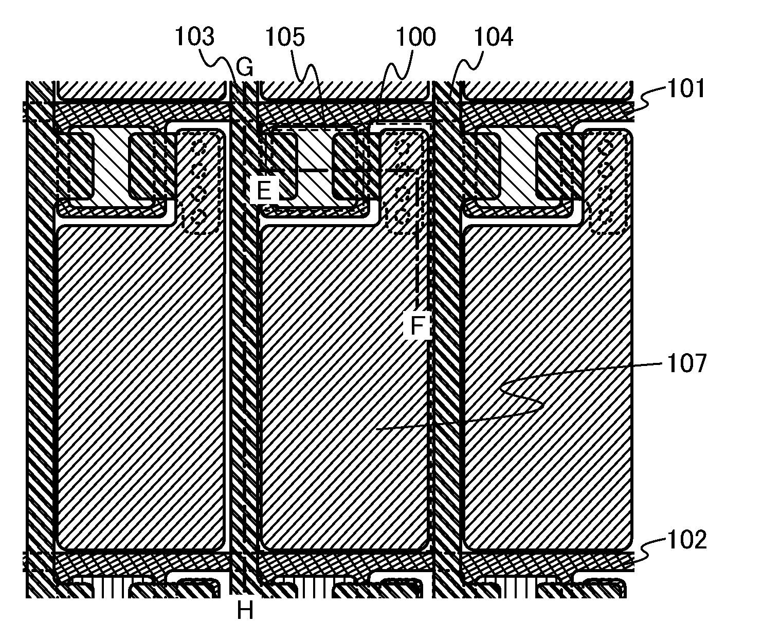
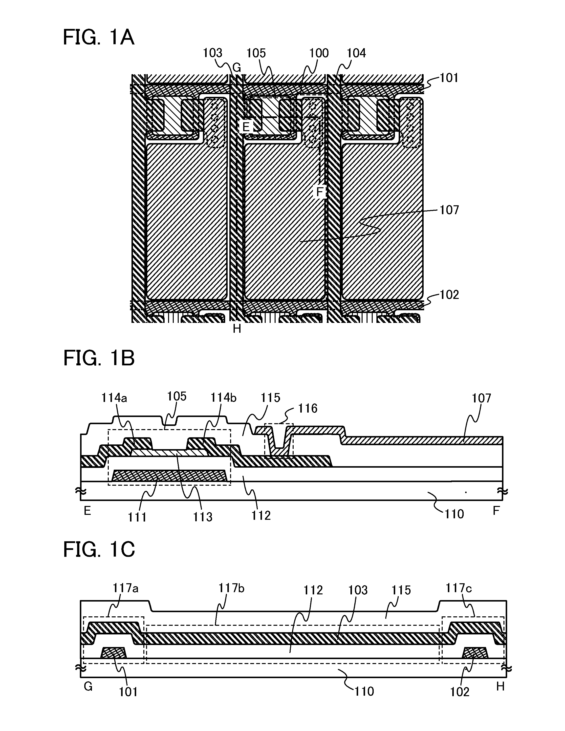
[0033]First, an example of a structure of a pixel included in a liquid crystal display device of one embodiment of the present invention is described with reference to FIGS. 1A to 1C. Specifically, an example of a structure of a pixel in a liquid crystal display device having a structure in which a liquid crystal material is interposed between one substrate provided with a pixel electrode and the other substrate provided with a counter electrode (a liquid crystal display device in w...
PUM
 Abstract
Description
Claims
Application Information