Method for manufacturing semiconductor device

a manufacturing method and semiconductor technology, applied in the direction of semiconductor devices, electrical appliances, transistors, etc., can solve the problems of increasing the power consumption of the semiconductor device, and achieve the effects of reducing the impurities remaining in the semiconductor layer, high reliability, and suppressing the variation of the threshold voltag

Inactive Publication Date: 2011-09-08
SEMICON ENERGY LAB CO LTD
View PDF130 Cites 61 Cited by
  • Summary
  • Abstract
  • Description
  • Claims
  • Application Information

AI Technical Summary

Benefits of technology

[0008]In a transistor which utilizes semiconductor characteristics, it is preferable that variation in threshold voltage caused by time degradation be small. This is because when a transistor whose variation in threshold voltage is large due to time degradation is used for a semiconductor device, the reliability of the semiconductor device is lowered. In addition, in a transistor which utilizes semiconductor characteristics, it is preferable that the off-state current be low. When a transistor whose off-state current is high is used for a semiconductor device, the power consumption of the semiconductor device is increased.
[0009]It is an object of the present invention to provide a method for manufacturing a highly reliable semiconductor device.
[0010]It is another object of the present invention to provide a method for manufacturing a semiconductor device with low power consumption.

Problems solved by technology

When a transistor whose off-state current is high is used for a semiconductor device, the power consumption of the semiconductor device is increased.

Method used


Image

  • Method for manufacturing semiconductor device
  • Method for manufacturing semiconductor device
  • Method for manufacturing semiconductor device

Examples


embodiment 1

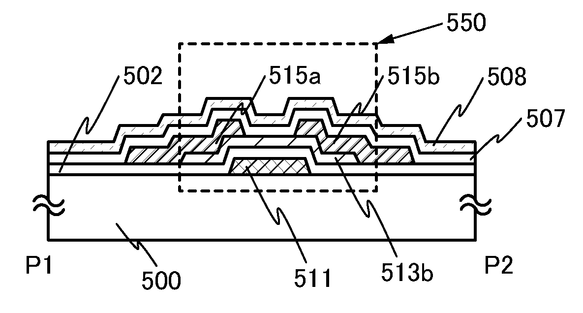
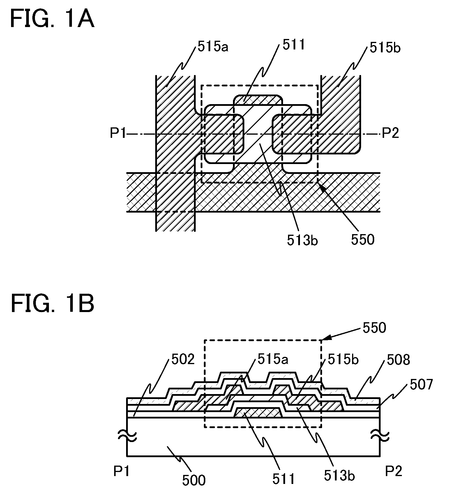
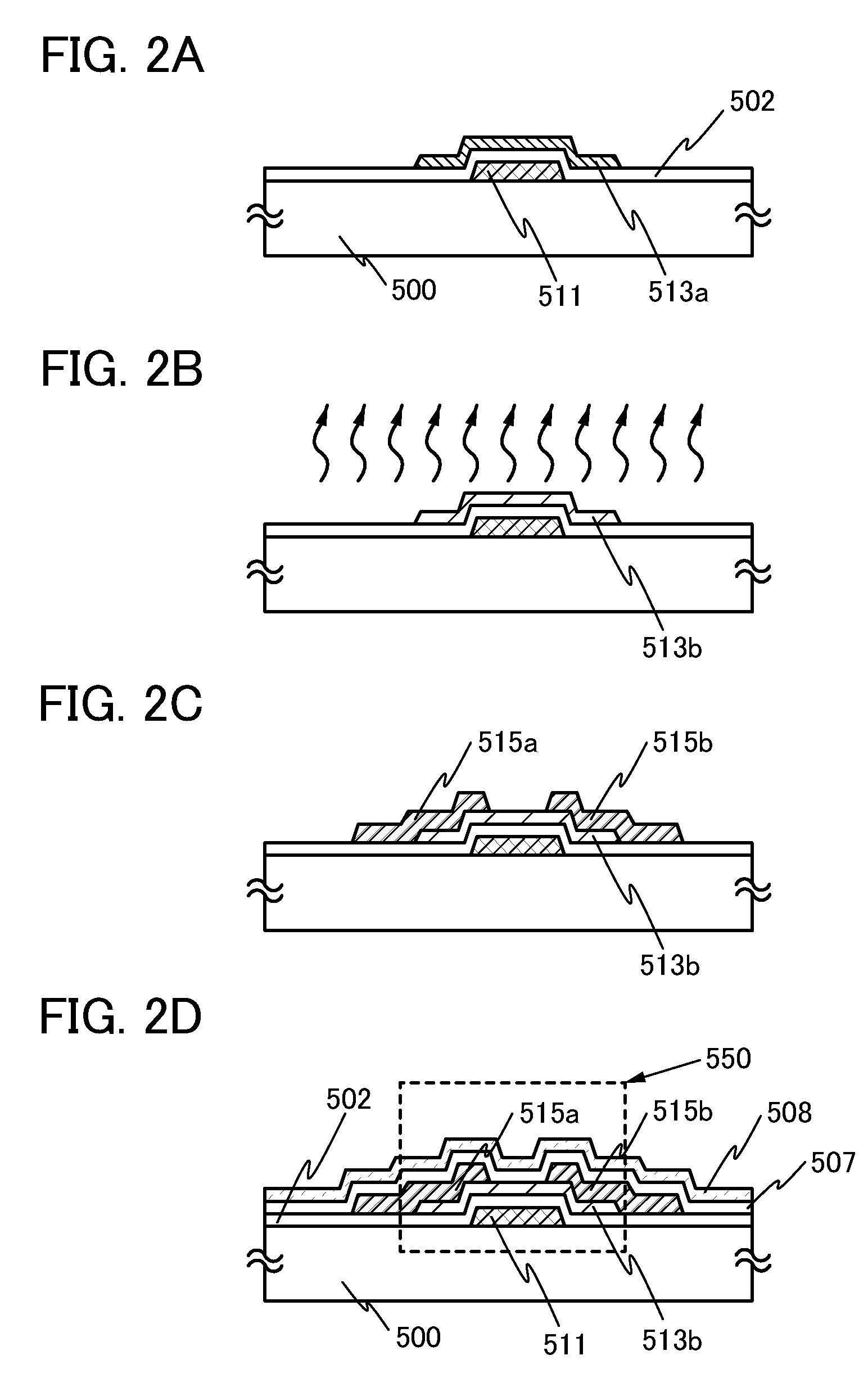
[0052]In this embodiment, a bottom-gate transistor which is manufactured by a method in which an oxide semiconductor layer is formed while a substance containing a halogen element is introduced into a film formation chamber in a gaseous state and is later subjected to heat treatment to form a highly purified oxide semiconductor layer, and a method for manufacturing the bottom-gate transistor will be described with reference to FIGS. 1A and 1B and FIGS. 2A to 2D.

[0053]FIGS. 1A and 1B illustrate a structure of a bottom-gate transistor 550 which is manufactured in this embodiment. FIG. 1A is a top view of the transistor 550, and FIG. 1B is a cross-sectional view of the transistor 550. Note that FIG. 1B corresponds to the cross-sectional view taken along a line P1-P2 in FIG. 1A.

[0054]In the transistor 550, a gate electrode 511 and a gate insulating layer 502 which covers the gate electrode 511 are provided over a substrate 500 having an insulating surface. A highly purified oxide semico...

embodiment 2

[0143]In this embodiment, a top-gate transistor which is manufactured by a method in which an oxide semiconductor layer is formed while a substance containing a halogen element is introduced into a film formation chamber in a gaseous state and is later subjected to heat treatment to form a highly purified oxide semiconductor layer, and a method for manufacturing the top-gate transistor will be described with reference to FIGS. 3A and 3B and FIGS. 4A to 4D.

[0144]FIGS. 3A and 3B illustrate a structure of a top-gate transistor 650 which is manufactured in this embodiment. FIG. 3A is a top view of the transistor 650, and FIG. 3B is a cross-sectional view of the transistor 650. Note that FIG. 3B corresponds to the cross-sectional view taken along a line Q1-Q2 in FIG. 3A.

[0145]In the transistor 650, over a substrate 600 having an insulating surface, a first electrode 615a and a second electrode 615b which each serve as a source or drain electrode are provided. A highly purified oxide semi...

embodiment 3

[0181]In this embodiment, a structure and a method for manufacturing a semiconductor device according to one embodiment of the present invention will be described with reference to FIGS. 5A and 5B, FIGS. 6A to 6D, FIGS. 7A to 7C, FIGS. 8A to 8D, and FIGS. 9A to 9C. Note that the semiconductor device described as an example in this embodiment can be used as a memory device.

[0182]A structure of a semiconductor device described as an example in this embodiment is illustrated in FIGS. 5A and 5B. FIG. 5A is a cross-sectional view of the semiconductor device, and FIG. 5B is a plan view of the semiconductor device. Note that FIG. 5A is a cross-sectional view taken along line A1-A2 and line B1-B2 in FIG. 5B.

[0183]The semiconductor device described as an example includes a transistor 260 including a first semiconductor material in a lower portion, a transistor 262 including a second semiconductor material in an upper portion, and a capacitor 264. A gate electrode 210 of the transistor 260 is...


PUM


Abstract

A highly purified oxide semiconductor layer is formed in such a manner that a substance that firmly bonds during film formation to an impurity containing a hydrogen atom is introduced into a film formation chamber, the substance is reacted with the impurity containing a hydrogen atom remaining in the film formation chamber, and the substance is changed to a stable substance containing the hydrogen atom. The stable substance containing the hydrogen atom is exhausted without providing a metal atom of an oxide semiconductor layer with the hydrogen atom; therefore, a phenomenon in which a hydrogen atom or the like is taken into the oxide semiconductor layer can be prevented. As the substance that firmly bonds to the impurity containing a hydrogen atom, a substance containing a halogen element is preferable, for example.

Description

TECHNICAL FIELD[0001]The present invention relates to a semiconductor device including an oxide semiconductor, and a method for manufacturing the semiconductor device. Note that here, semiconductor devices refer to general elements and devices which function utilizing semiconductor characteristics.BACKGROUND ART[0002]A technique in which a transistor is formed using a semiconductor layer formed over a substrate having an insulating surface is known. For example, a technique in which a transistor is formed over a glass substrate using a thin film containing a silicon-based semiconductor material and applied to a liquid crystal display device and the like is known.[0003]A transistor which is used in a liquid crystal display device is generally formed using a semiconductor material such as amorphous silicon or polycrystalline silicon. Although transistors including amorphous silicon have low field effect mobility, they can be formed over a larger glass substrate. Meanwhile, although tr...

Claims


Application Information

Patent Timeline
Patent Type & Authority Applications(United States)
IPC IPC(8): H01L29/786H01L21/34
CPCH01L27/1203H01L27/1225H01L29/7869H01L21/02554H01L27/1156H01L21/02631H01L21/02667H01L21/3228H01L27/11521H01L21/02565H10B41/30H10B41/70H01L29/66742
Inventor YAMAZAKI, SHUNPEISUZUKI, KUNIHIKO
Owner SEMICON ENERGY LAB CO LTD
Why Eureka
Try Eureka