Semiconductor cells, arrays, devices and systems having a buried conductive line and methods for forming the same

a technology of conductive lines and semiconductor cells, applied in semiconductor devices, diodes, electrical apparatus, etc., can solve the problems of increasing substrate bias effect, reducing current drivability and reliability degradation, and increasing substrate bias

Active Publication Date: 2011-09-08
OVONYX MEMORY TECH LLC
View PDF96 Cites 59 Cited by
  • Summary
  • Abstract
  • Description
  • Claims
  • Application Information

AI Technical Summary

Problems solved by technology

However, there are several drawbacks to shrinking planar transistors 16 in access devices 12 of DRAM arrays 10, such as threshold voltage variation, short-channel effect (“SCE”), increase of substrate-bias effect due to impurity concentration enhancement in the channel region, and reliability degradation by hot-carriers.
The narrow width transistors also cause decrease of current drivability and reliability degradation.
The high parasitic resi

Method used


Image

  • Semiconductor cells, arrays, devices and systems having a buried conductive line and methods for forming the same
  • Semiconductor cells, arrays, devices and systems having a buried conductive line and methods for forming the same
  • Semiconductor cells, arrays, devices and systems having a buried conductive line and methods for forming the same

Examples


Embodiment Construction

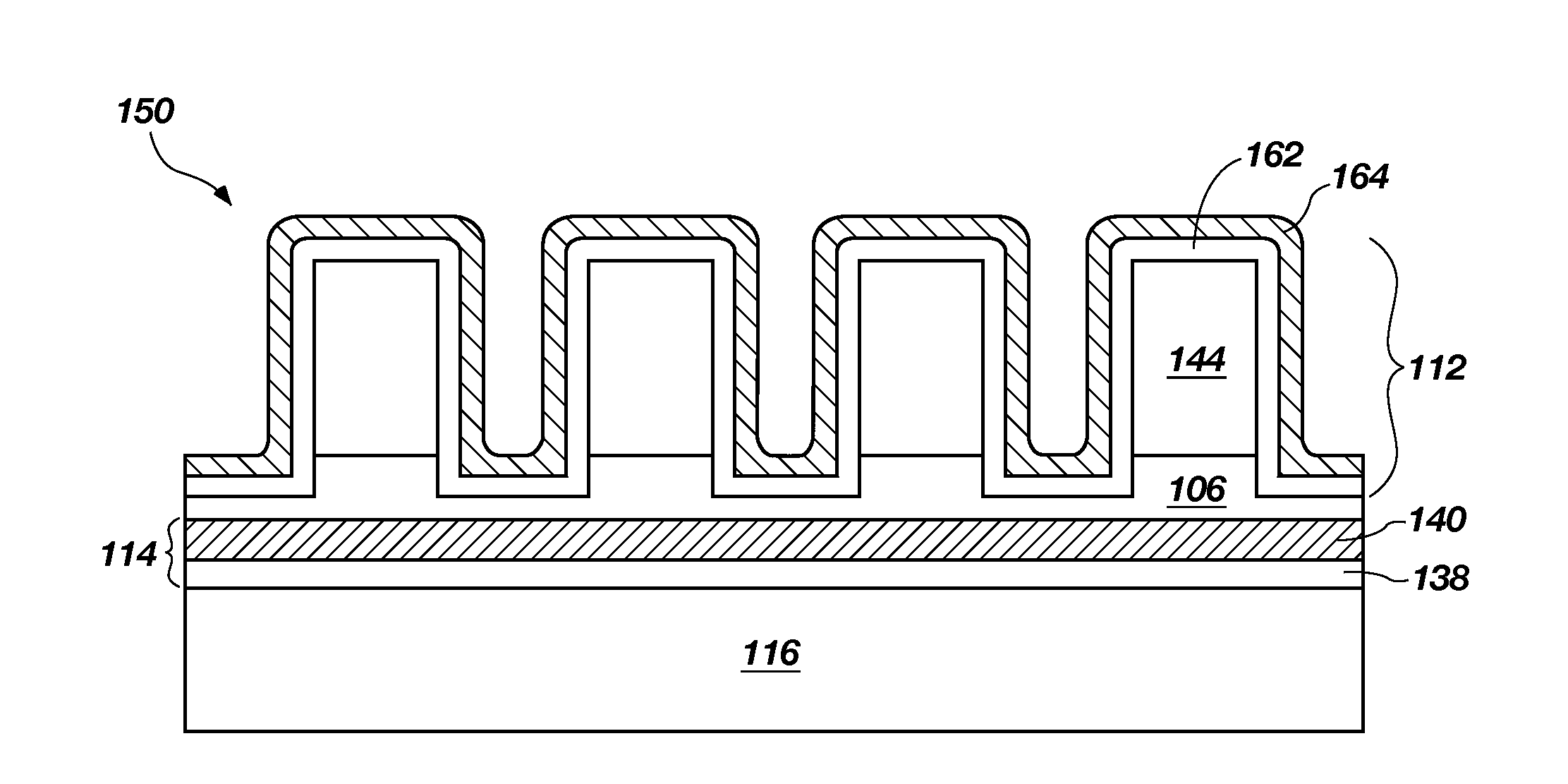
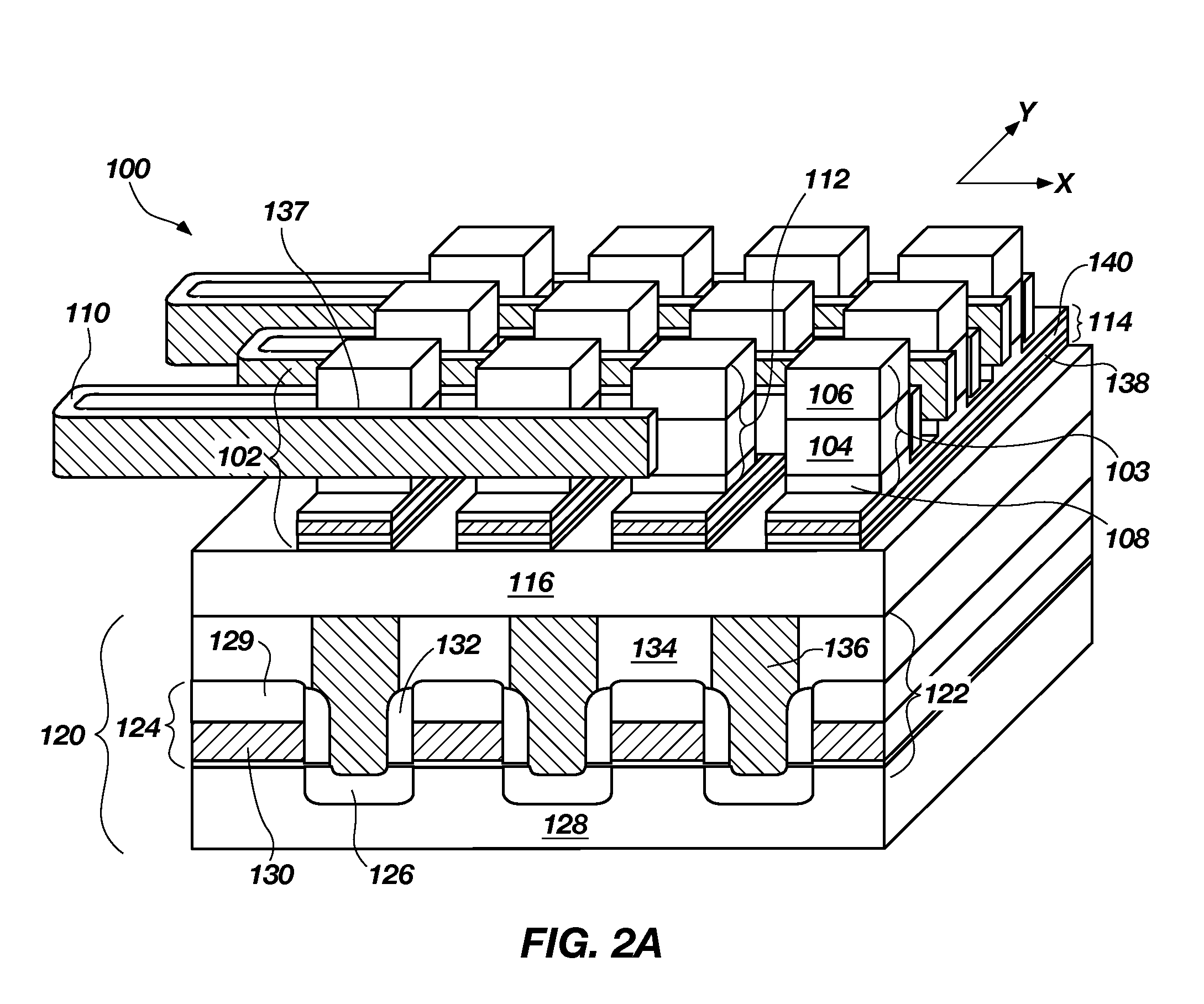
Access devices, semiconductor devices and electrical systems including such access devices and methods for forming such access devices, devices and systems are disclosed. Such access devices include, for example, at least one transistor disposed on a conductive line and including a channel region interposed between a drain region and a source region. The access devices may further include an access line associated with the transistor. As used herein, the term “interposed” means and includes disposed between or situated between elements in such a manner that perimeters or outer surfaces thereof generally coincide. The conductive line may function as a data / sense line and provide an electrical connection to the transistor. The access devices may have a cell size of 4F2, wherein F is a minimum feature size, to provide semiconductor devices having improved scalability, reduced area and increased access device density. An upper region of the transistors may remain exposed for electrical ...


PUM


Abstract

Semiconductor arrays including a plurality of access devices disposed on a buried conductive line and methods for forming the same are provided. The access devices each include a transistor having a source region and drain region spaced apart by a channel region of opposite dopant type and an access line associated with the transistor. The access line may be electrically coupled with one or more of the transistors and may be operably coupled to a voltage source. The access devices may be formed in an array on one or more conductive lines. A system may be formed by integrating the semiconductor devices with one or more memory semiconductor arrays or conventional logic devices, such as a complementary metal-oxide-semiconductor (CMOS) device.

Description

TECHNICAL FIELDEmbodiments of the present invention relate to semiconductor cells, arrays, devices and systems having substantially enhanced scalability, density and integration capacity and methods for forming such semiconductor devices.BACKGROUNDMemory devices are typically provided as internal, semiconductor, integrated circuits in computers or other electronic devices. There are many different types of memory including random-access memory (RAM), read only memory (ROM), synchronous dynamic random access memory (SDRAM), dynamic random access memory (DRAM), and non-volatile memory. The trend in the semiconductor industry is toward smaller memory devices that may be used to fabricate high density circuits on a single chip. The miniaturization of transistor devices and circuits may be achieved by reducing the size of all the features of surface-oriented devices so that the resultant devices occupy a smaller surface area of a wafer.FIG. 1 illustrates a conventional DRAM array 10 incl...

Claims


Application Information

Patent Timeline
IPC IPC(8): H01L29/78H01L21/336
CPCH01L29/78H01L29/66666H01L27/108H01L29/7827H10B63/34H10B63/82H10N70/231H10N70/826H10N70/8828H10B12/31H10B12/00H01L21/32H01L21/762H01L27/0814H01L29/861
Inventor TANG, SANH D.ZAHURAK, JOHN K.
Owner OVONYX MEMORY TECH LLC
Why Eureka
Try Eureka