Piezoelectric film, piezoelectric device, liquid ejection apparatus, and method of producing piezoelectric film

a piezoelectric film and liquid ejection technology, applied in the field of piezoelectric film, piezoelectric device, liquid ejection apparatus, and method of producing piezoelectric film, can solve the problems of arcing phenomenon, inability to make films thick, and ineffective lamination and crystallization formation of horizontal stripes, so as to achieve the effect of improving driving durability, preventing effective lamination and crystallization, and improving driving durability

Inactive Publication Date: 2011-09-08
FUJIFILM CORP
View PDF4 Cites 10 Cited by
  • Summary
  • Abstract
  • Description
  • Claims
  • Application Information

AI Technical Summary

Benefits of technology

[0035]According to these aspects of the present invention, the formation of the horizontal stripes caused by the repetition of the lamination and crystallization can be prevented effectively, and the piezoelectric film having the columnar crystal structure can be obtained. According to the piezoelectric film of the present invention, the normal of the (100) plane of each of the crystals constituting the piezoelectric film is inclined by a predetermined angle with respect to the normal direction of the surface of the substrate, in which is a driving electric field is applied. Therefore, the driving durability can be improved. Moreover, the use of the vapor deposition process can produce a thick piezoelectric film without causing cracks. The driving durability can be further improved since no irregular lamination occurs and formation of defects due to use of the piezoelectric film can be prevented.

Problems solved by technology

However, in a PZT (lead titanate zirconate) film in the related art, leakage associated with grain boundaries and formation of defects occur during continuous driving of the PZT film, causing insulation breakdown.
Moreover, it is known that a large amount of Pb (lead) in the PZT film easily induces migration of Pb ions in the course of repeatedly applying the drive voltage, causing an arcing phenomenon.
The piezoelectric device described in Japanese Patent Application Publication No. 11-307833 is produced exclusively by a sol-gelation process; however, the problems in producing piezoelectric devices using the sol-gelation process include not being able to make films thick, irregular composition in the depth direction of the films, and poor production efficiency (slow film formation speed).
However, producing a PZT film of at least 2 μm thickness by using the sol-gelation process might cause cracks on the PZT film, due to thermal stress resulting from a repetition of coating and sintering steps.
Therefore, it is difficult to produce a PZT film of at least 2 μm thickness by using the sol-gelation process.
Moreover, use of the sol-gelation process to produce a PZT film causes horizontal stripes each time sintering crystallization is performed, and when piezoelectric crystals repeatedly perform the functions associated with the piezoelectric effects, the stripe defects originate cracks, resulting in lowering the durability.

Method used


Image

  • Piezoelectric film, piezoelectric device, liquid ejection apparatus, and method of producing piezoelectric film
  • Piezoelectric film, piezoelectric device, liquid ejection apparatus, and method of producing piezoelectric film
  • Piezoelectric film, piezoelectric device, liquid ejection apparatus, and method of producing piezoelectric film

Examples


example 1

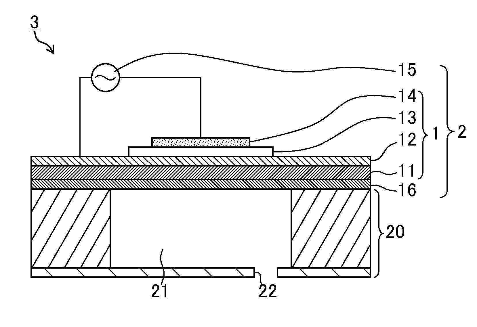
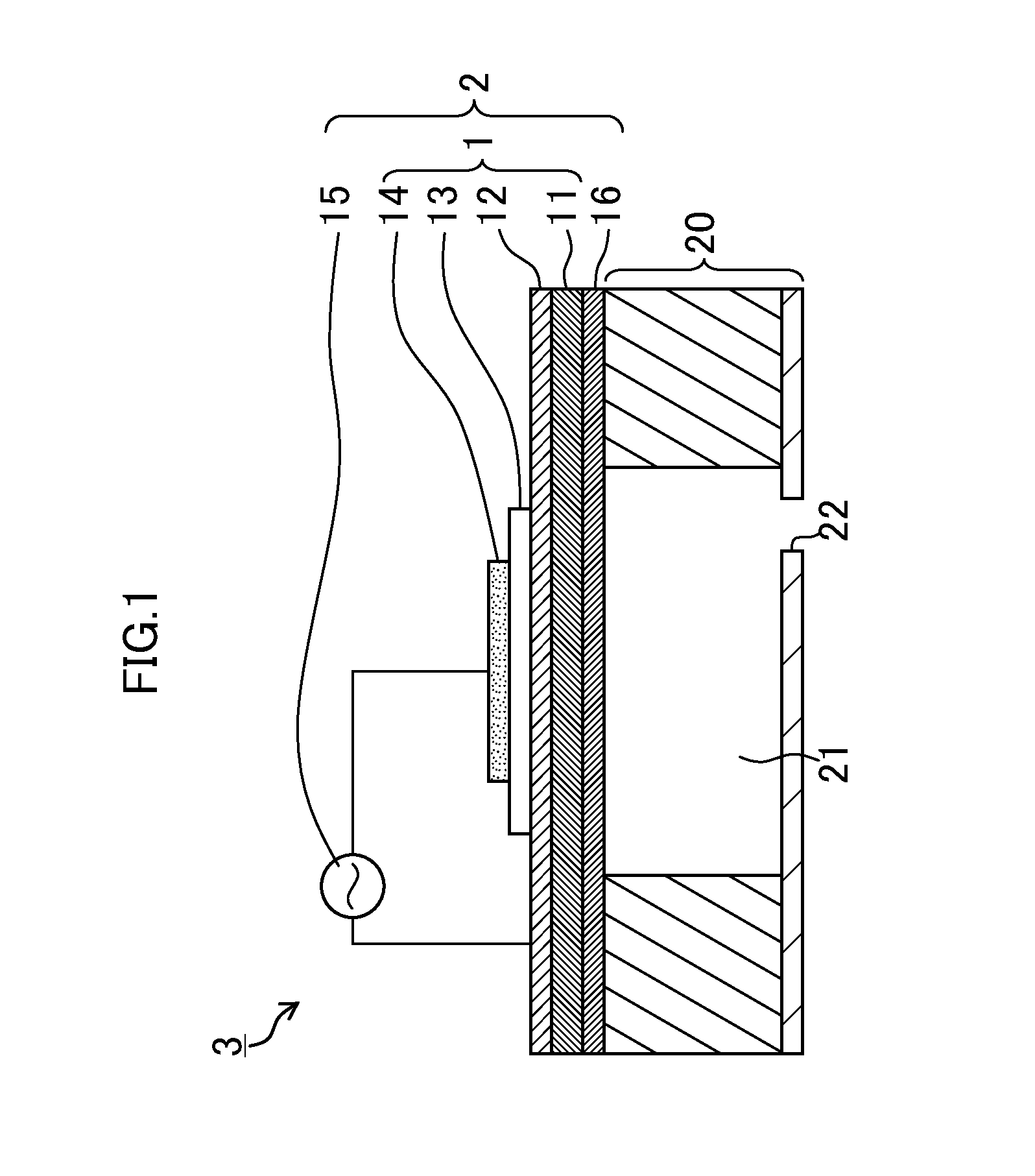
[0104]A Ti film with a thickness of 30 nm and an Ir film with a thickness of 150 nm were sequentially formed on an SOI substrate to obtain a lower electrode, by using the sputtering method at the substrate temperature of 350° C. A Nb-doped PZT piezoelectric film with a thickness of 4 um was formed on this lower electrode. This film formation was performed under the following conditions.

>

[0105]Film formation apparatus: RF sputtering apparatus

Target: Pb1.3((Zr0.52Ti0.48)0.88Nb0.12)O3 sintered body (the amount of Nb occupying the B-site: 12 mol %)

Substrate temperature: 475° C.

Target-substrate (T-S) distance: 60 mm

Film formation pressure: 0.30 Pa

Film formation gas: Ar / O2=97.5 / 2.5 (molar ratio)

Substrate potential Vsub=−12 V

The substrate potential Vsub was set at +25 V for five minutes after starting the film formation in order to provide a perovskite layer as an initial layer.

[0106]As a result of performing the XRD measurement to examine the orientation of the piezoelectric film after co...

examples 2 to 6

[0112]The same method as that of Example 1 was used for producing piezoelectric films and inkjet recording heads under the conditions described in FIG. 5, and the obtained piezoelectric films and inkjet recording heads were evaluated.


PUM

PropertyMeasurementUnit
thicknessaaaaaaaaaa
thicknessaaaaaaaaaa
thicknessesaaaaaaaaaa

Abstract

A piezoelectric film is formed on a surface of a substrate by a vapor deposition process without generating grain boundaries which are substantially parallel to the surface of the substrate and are caused by lamination. A normal of a (100) plane of each of crystals constituting the piezoelectric film is inclined from a normal of the surface of the substrate by an angle of not smaller than 6° and not larger than 36°.

Description

BACKGROUND OF THE INVENTION[0001]1. Field of the Invention[0002]The present invention relates to a piezoelectric film, a piezoelectric device, a liquid ejection apparatus, and a method of producing a piezoelectric film, more particularly to a piezoelectric film with improved durability in continuous driving, a piezoelectric device including the piezoelectric film, a liquid ejection apparatus including the piezoelectric device, and a method of producing the piezoelectric film.[0003]2. Description of the Related Art[0004]There has been known a piezoelectric device that is obtained by combining a piezoelectric film having a piezoelectric property displaced by application of a drive voltage, with electrodes through which the drive voltage is applied to the piezoelectric film Japanese Patent Application Publication No. 11-307833, for example, describes a piezoelectric device in which the (100) orientation in the crystal forming a piezoelectric film is inclined by 5° to 20°. Inclining the...

Claims


Application Information

Patent Timeline
Patent Type & Authority Applications(United States)
IPC IPC(8): H01L41/04H01L41/08H01L41/18B32B5/00B05D5/12C23C14/48C23C14/34B41J2/045B41J2/055B41J2/135B41J2/14B41J2/16C23C14/08C23C16/40H01L41/09H01L41/187
CPCB41J2/14233H01L41/0805H01L41/0973H01L41/1876B41J2/1646B41J2/1612B41J2/1642B41J2/1645H01L41/316H10N30/1051H10N30/2047H10N30/8554H10N30/076
Inventor NAONO, TAKAYUKI
Owner FUJIFILM CORP
Why Eureka
Try Eureka