Manufacturing method of gallium oxide single crystal

a manufacturing method and single crystal technology, applied in the direction of single crystal growth, polycrystalline material growth, eutectoid material demixing, etc., can solve the problems of high cost of manufacturing gallium oxide, high binding energy, and high heat energy for breaking the atomic bonds of gallium oxid

Inactive Publication Date: 2011-09-15
SEMICON ENERGY LAB CO LTD
View PDF85 Cites 5 Cited by
  • Summary
  • Abstract
  • Description
  • Claims
  • Application Information

AI Technical Summary

Benefits of technology

[0011]Consequently, there is a problem that cost of manufacturing gallium oxide is high. An object of an embodiment of the present invention is to provide a method of growing a single crystal of gallium oxide at a lower temperature than the melting point (1900° C.) of gallium oxide.
[0012]To form a crystal lattice of gallium oxide from an amorphous state, it is necessary to break bonds between oxygen atoms and gallium atoms and then rearrange the oxygen atoms and the gallium atoms. Therefore, it is necessary to add energy for breaking the bonds between the oxygen atoms and the gallium atoms from the outside. Gallium oxide has a large bandgap of about 5 eV, which originates from the atoms of gallium oxide having high binding energy. Consequently, heat energy for breaking the atomic bonds of gallium oxide is high.
[0013]However, in a gallium oxide compound containing atoms or molecules that easily sublimate, if oxygen atoms or gallium atoms are bonded to the atoms or molecules that easily sublimate, the atoms or molecules sublimate easily from inside the gallium oxide by adding from the outside a heat energy that is lower than the binding energy, and after they sublimate, a dangling bonds of the oxygen atoms and the gallium atoms occur. With this, rearrangement of the oxygen atoms and the gallium atoms becomes easy, and it is possible to generate crystallization of gallium oxide with lower energy than the binding energy.

Problems solved by technology

Consequently, there is a problem that cost of manufacturing gallium oxide is high.

Method used


Image

  • Manufacturing method of gallium oxide single crystal
  • Manufacturing method of gallium oxide single crystal
  • Manufacturing method of gallium oxide single crystal

Examples


embodiment 1

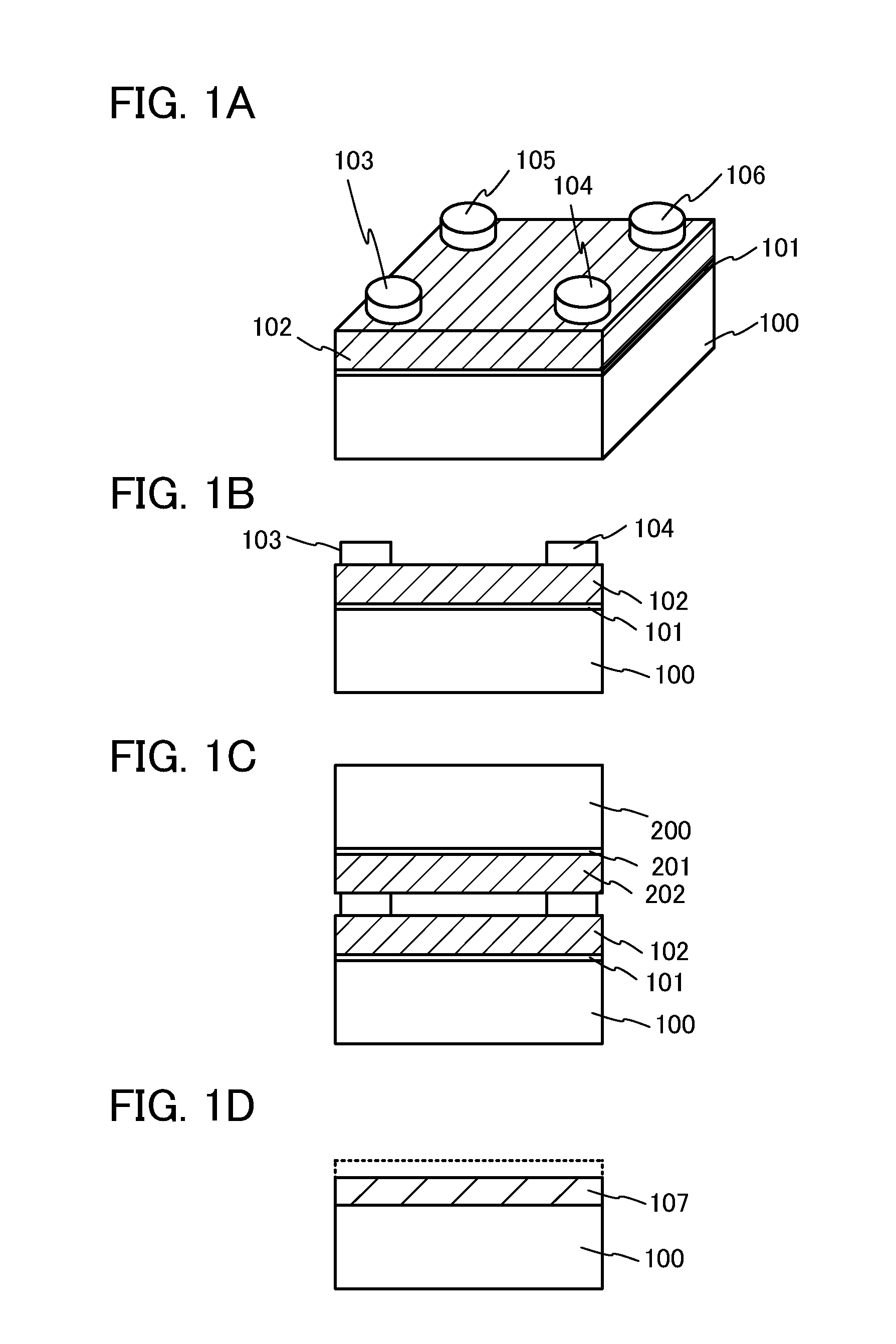
[0032]In this embodiment, an example of a method of obtaining a single crystal of gallium oxide will be described below with reference to FIGS. 1A to 1D.

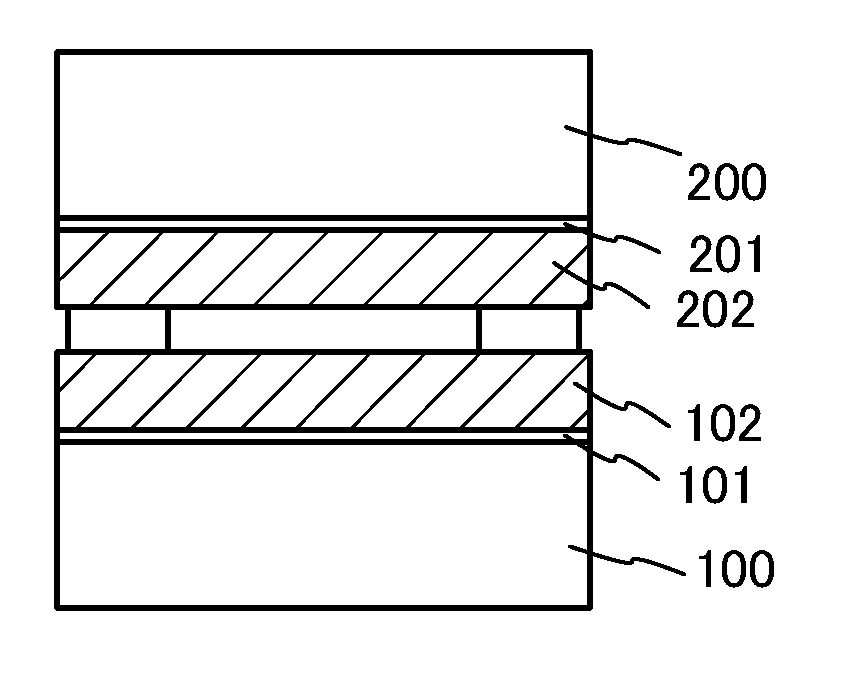
[0033]First, a first metal oxide film 101 and a first gallium oxide compound film 102 are formed and laminated over a first single crystal substrate 100.

[0034]As the first metal oxide film 101, a zinc oxide film that is obtained by a sputtering method is used, and the film thickness is to be 1 nm or more and 10 nm or less.

[0035]As the first gallium oxide compound film 102, an InGaO film, an InGaZnO film, a GaZnO film, or the like that is obtained by a sputtering method can be used, and the film thickness is to be 10 nm or more and 500 nm or less.

[0036]Then, spacing materials 103, 104, 105, and 106 are placed at four corners of the first gallium oxide compound film 102 over the first single crystal substrate 100, to maintain substrate spacing. A perspective view at this stage corresponds to FIG. 1A, and a corresponding cross-sectiona...

example 1

[0046]In this example, as each of the first single crystal substrate and the second single crystal substrate, an yttria-stabilized zirconia substrate with a plane orientation of (1 1 1), which is a so-called YSZ substrate (substrate size of 10 mm×10 mm, thickness of 0.5 mm), is used.

[0047]Over each of the first single crystal substrate and the second single crystal substrate, a zinc oxide film with a film thickness of 2 nm and an InGaZnO film with a film thickness of 100 nm were laminated.

[0048]Formation of the zinc oxide film was performed with a film formation pressure of 0.4 Pa, a power of 0.5 kW, an argon flow rate of 10 sccm, and an oxygen flow rate of 5 sccm.

[0049]Formation of the InGaZnO film was performed using an oxide target of In2O3:Ga2O3:ZnO=1:1:1 [molar ratio], with a film formation pressure of 0.4 Pa, a power of 0.5 kW using a DC power source, an argon flow rate of 10 sccm, and an oxygen flow rate of 5 sccm. The InGaZnO film immediately after being formed is an amorpho...

example 2

[0059]In this example, a result of performing an experiment under conditions with different target composition ratio and heat treatment temperature from those in Example 1 will be described. Note that, other conditions are the same as those in Example 1; therefore, descriptions there will be omitted.

[0060]In this example, an InGaZnO film was formed using an oxide target of In2O3:Ga2O3:ZnO=1:1:10 [molar ratio], with a film formation pressure of 0.4 Pa, a power of 0.5 kW using a DC power source, an argon flow rate of 10 sccm, and an oxygen flow rate of 5 sccm. Note that the InGaZnO film immediately after being formed is an amorphous film.

[0061]Also, a maintained temperature of the heating treatment was set at 1350° C. A cross-sectional TEM image of a single crystal layer of gallium oxide obtained by the heating treatment is shown in FIG. 6. It can be observed that lattice images are lined up horizontally and that a single crystal is growing.

[0062]FIG. 7 shows a result of an EDX analys...


PUM

PropertyMeasurementUnit
temperatureaaaaaaaaaa
melting pointaaaaaaaaaa

Abstract

A method of growing a single crystal of gallium oxide at a lower temperature than the melting point (1900° C.) of gallium oxide is provided. A compound film (hereinafter referred to as “gallium oxide compound film”) containing Ga atoms, O atoms, and atoms or molecules that easily sublimate, is heated to sublimate the atoms or molecules that easily sublimate from inside the gallium oxide compound film, thereby growing a single crystal of gallium oxide with a heat energy that is lower than a binding energy of gallium oxide.

Description

BACKGROUND OF THE INVENTION[0001]1. Field of the Invention[0002]The present invention relates to a manufacturing method of a metal oxide single crystal, for example, a gallium oxide single crystal, and specifically relates to a method of obtaining a gallium oxide single crystal layer by growing a gallium oxide single crystal over a single crystal substrate that is not gallium oxide.[0003]2. Description of the Related Art[0004]Because gallium oxide single crystals (β type) have excellent light transmittance and have a large bandgap of about 5 eV (see Non-Patent Document 1, Non-Patent Document 2, and Non-Patent Document 3), they are expected as application materials for devices that operate stably under a high temperature, deep ultraviolet sensors, light-emitting devices, or the like. Also, manufacturing of a gallium oxide single crystal is described in Patent Document 1 and Patent Document 2.REFERENCE[Patent Document][0005][Patent Document 1] Japanese Published Patent Application No....

Claims


Application Information

Patent Timeline
Patent Type & Authority Applications(United States)
IPC IPC(8): C30B1/02
CPCC30B29/16C30B1/04
Inventor MIYANAGA, AKIHARUHONDA, TATSUYAOMATA, TAKATSUGUNONAKA, YUSUKE
Owner SEMICON ENERGY LAB CO LTD
Why Eureka
Try Eureka