

Biaxial Strained Field Effect Transistor Devices
a transistor and field effect technology, applied in semiconductor devices, semiconductor/solid-state device details, electrical devices, etc., can solve problems such as channel mobility reduction
- Summary
- Abstract
- Description
- Claims
- Application Information
AI Technical Summary
Benefits of technology
Problems solved by technology
Method used
Image

Examples
Embodiment Construction
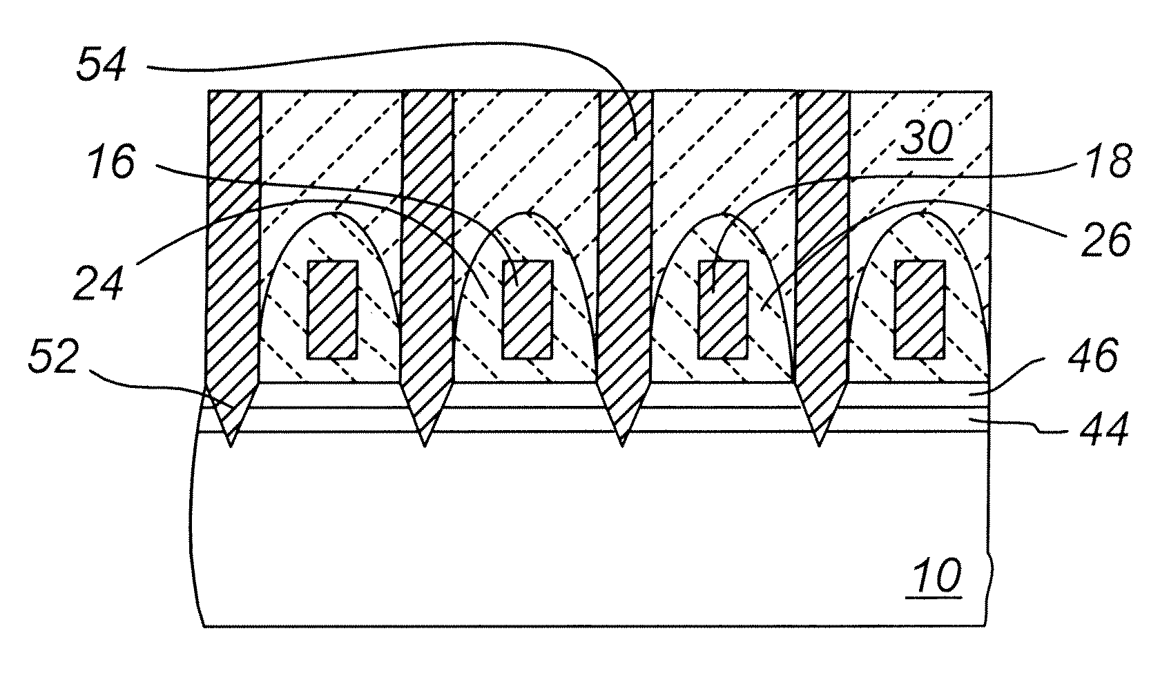
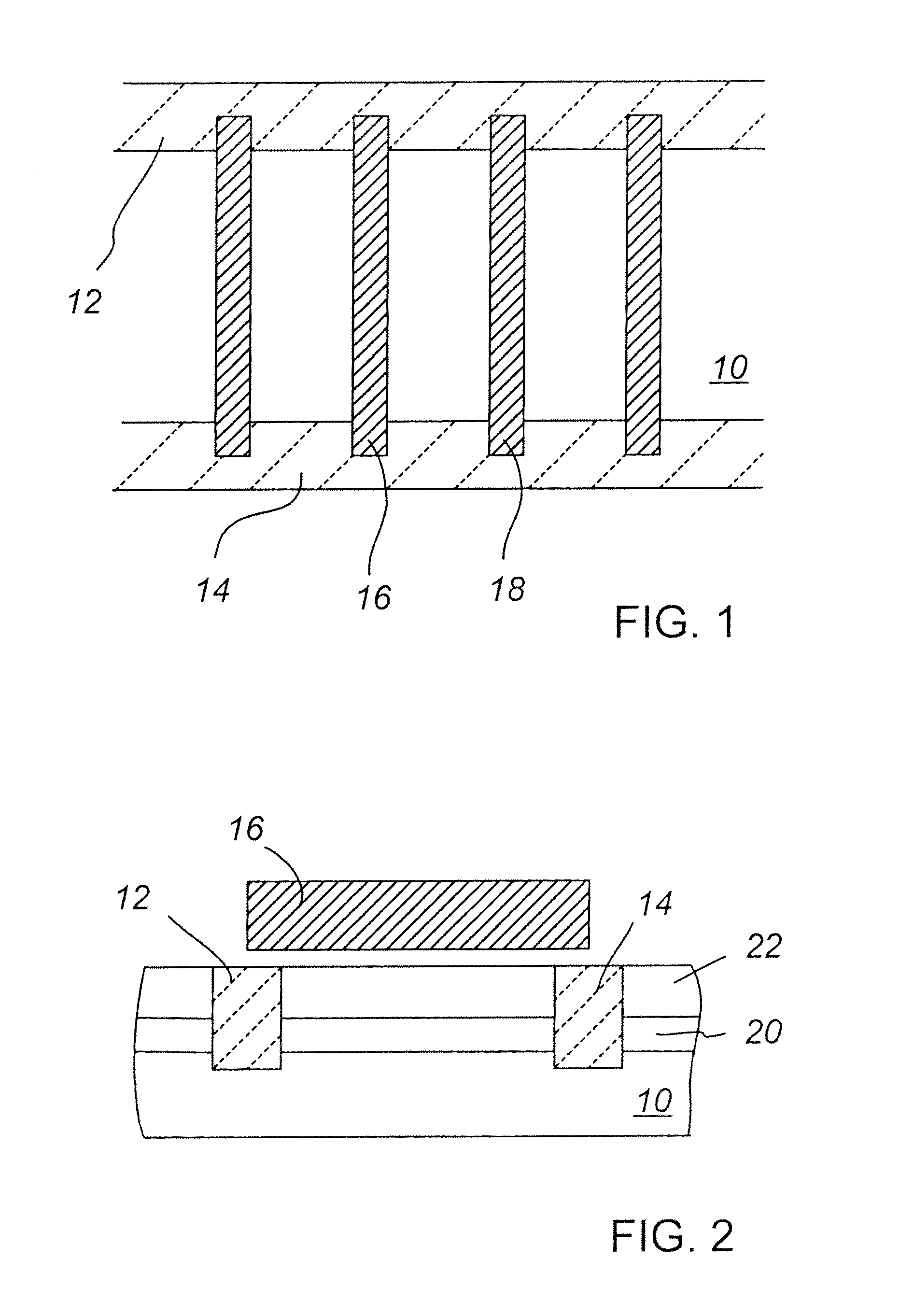
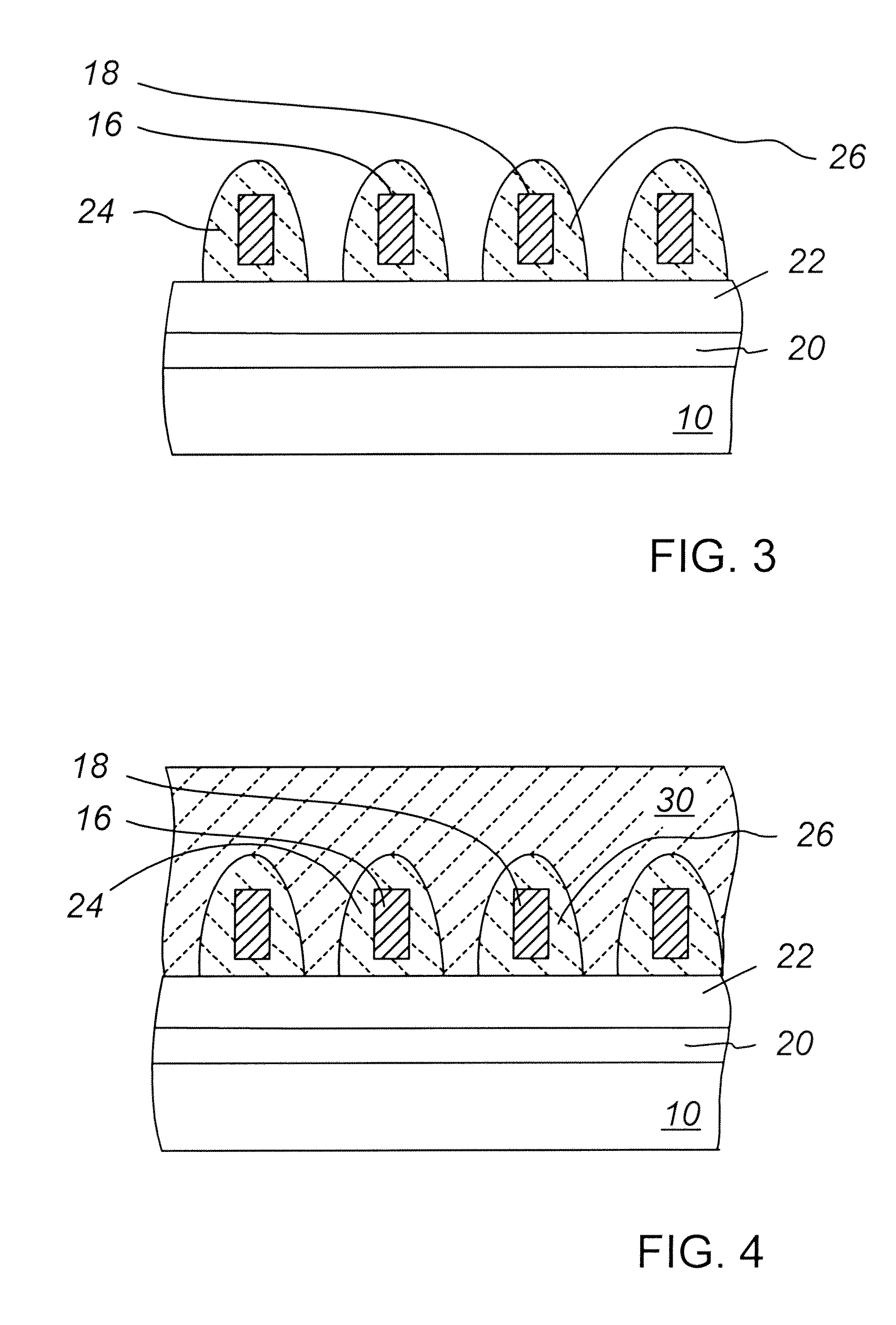
[0009]Aspects of the present invention provide a method of manufacturing a semiconductor device comprising providing a substrate having a semiconductor surface layer. A substrate has a semiconductor surface layer and a stressor layer positioned at a depth within the substrate and positioned adjacent the semiconductor surface layer. The buried stressor layer is in a stressed state in comparison to the semiconductor surface layer. A field effect transistor is formed on the semiconductor surface layer, with the field effect transistor comprising source and drain regions and a gate structure. A pre-metal dielectric layer is deposited over the field effect transistor. Openings are etched through the pre-metal dielectric layer to expose contact portions of the substrate on either side of the gate structure corresponding to portions of the source and drain of the field effect transistor. The method continues by etching into the substrate within the openings in the pre-metal dielectric, the...
PUM
 Abstract
Description
Claims
Application Information