Power semiconductor device and power conversion system using the device

a technology of power semiconductor and power conversion system, which is applied in the direction of power conversion system, amplifier with semiconductor device/discharge tube, amplifier with min 3 electrodes or 2 pn junctions, etc., can solve the problems of excessive surge voltage at a time of switching action, increase in the size of power semiconductor modules, increase in wire inductance, etc., to reduce the value of surge voltage, reduce the inductance of wires, and reduce the effect of power semiconductor modules

Active Publication Date: 2011-10-06
FUJI ELECTRIC CO LTD
View PDF5 Cites 32 Cited by
  • Summary
  • Abstract
  • Description
  • Claims
  • Application Information

AI Technical Summary

Benefits of technology

By applying the modules of the invention, it is possible to reduce the wire inductance between the direct current unit circuit and power semiconductor modules in a multi-level conversion system that converts power from an alternating current to a direct current, or from a direct current to an alternating current, and it is possible to considerably curb the value of the surge voltage occurring when the IGBT

Problems solved by technology

When the wires between the semiconductor modules and the direct current power source are long, as heretofore described, a problem occurs in that wire inductance increases, and a surge voltage at a time of a switching action becomes excessive.
Normally, a chip with a high amount of voltage resistance is such that th

Method used


Image

  • Power semiconductor device and power conversion system using the device
  • Power semiconductor device and power conversion system using the device
  • Power semiconductor device and power conversion system using the device

Examples


working example 1

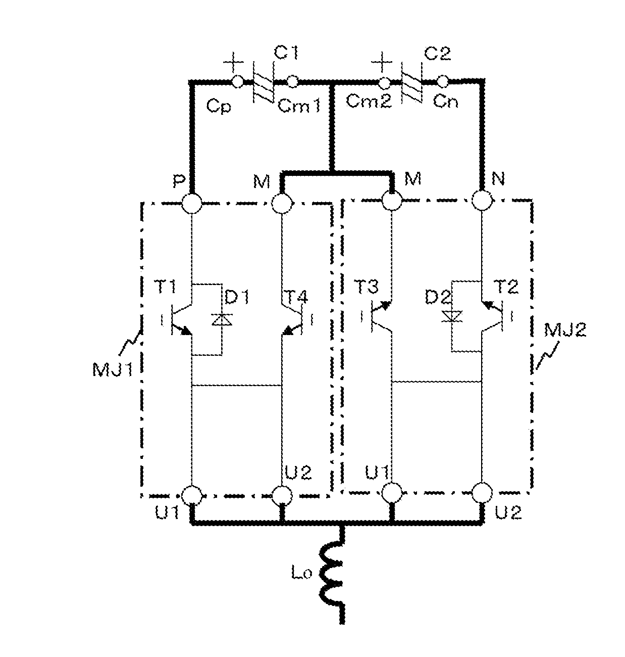
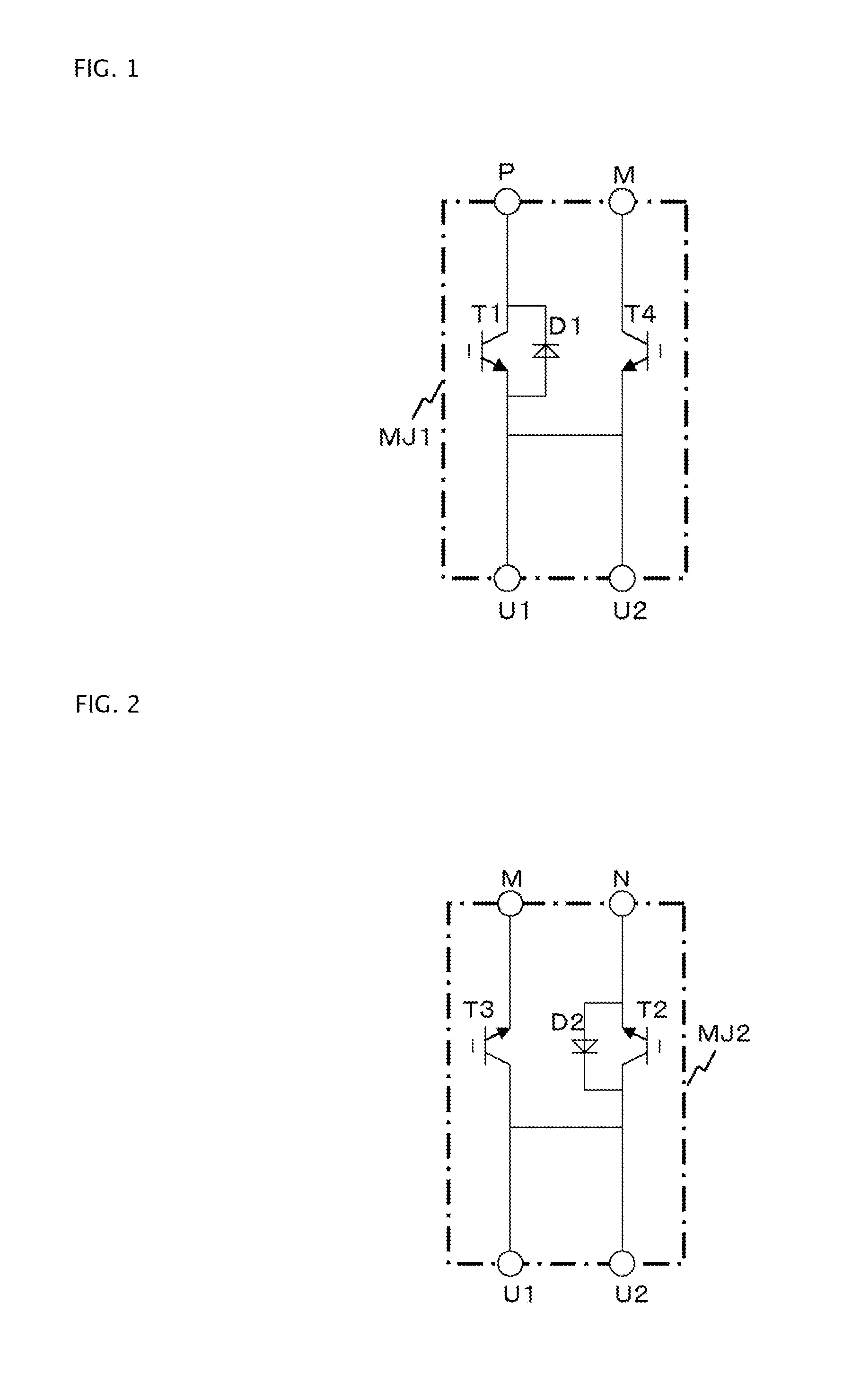
FIGS. 1 and 2 show a first working example of the invention. FIGS. 1 and 2 corresponding to first and second aspects of the invention respectively, a semiconductor element connected to a potential Cm of a direct current power source is an IGBT having reverse blocking voltage, and the shape of the module is that of the type of module in FIG. 20B. FIGS. 9 and 10 are a working example when the modules are applied to a three level inverter (a converter from a direct current to an alternating current). A module MJ1 of FIG. 1, incorporating an IGBT T1 to which a diode D1 is reverse parallel connected and a bidirectional switch reverse blocking type IGBT T4, is of a configuration wherein the IGBT T1 collector is connected to a terminal P, the reverse blocking type IGBT T4 collector to a terminal M, and connection points of the reverse blocking type IGBT T4 emitter and IGBT T1 emitter to terminals U (U1 and U2).

A module MJ2 of FIG. 2, incorporating an IGBT T2 to which a diode D2 is reverse ...

working example 2

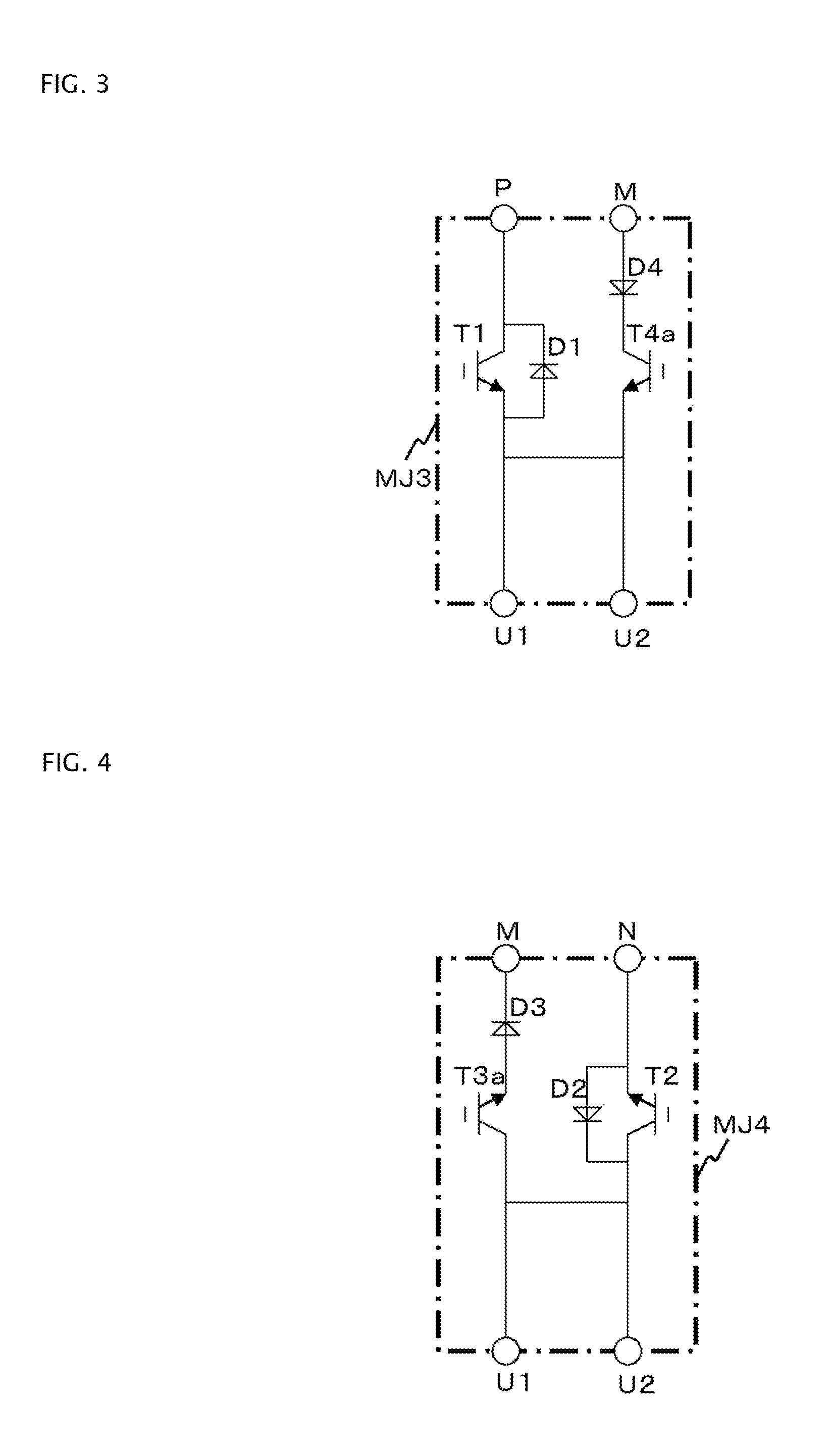
FIGS. 3 and 4 show a second working example of the invention. FIGS. 3 and 4 corresponding to third and fourth aspects of the invention respectively, the difference from the first working example is that the element connected to a potential Cm is an IGBT that does not have reverse blocking voltage. As bidirectional switch IGBTs T3a and T4a do not have reverse blocking voltage, diodes D3 and D4 are connected in series with the T3a and T4a respectively. Also, the shape of the module is that of the type of module in FIG. 20B.

A main circuit configuration and action when applying the modules to a three level inverter (a converter from a direct current to an alternating current) are the same as in FIGS. 9, 10 and 11A to 11D (ninth and eleventh aspects of the invention). Also, the functions are the same even in the event that the series connection order of the diode D3 and IGBT T3a, and of the diode D4 and IGBT T4a, are reversed. It is also possible to apply the modules in the same way to a...

working example 3

FIGS. 5 and 6 show a third working example of the invention. FIGS. 5 and 6 corresponding to fifth and sixth aspects of the invention respectively, IGBTs T3 and T4 connected to a potential Cm are elements having reverse blocking voltage, and the shape of the module is that of the type of module in FIG. 20B. FIGS. 12 and 13 show a working example when the modules are applied to a three level converter (a converter from an alternating current to a direct current).

A module MJ5 of FIG. 5, incorporating an IGBT T1 to which a diode D1 is reverse parallel connected and a reverse blocking type IGBT T3, is of a configuration wherein the IGBT T1 collector is connected to a terminal P, the IGBT T3 emitter to a terminal N, and connection points of the IGBT T1 emitter and IGBT T3 collector to terminals U (U1 and U2).

A module MJ6 of FIG. 6, incorporating an IGBT T2 to which a diode D2 is reverse parallel connected and a reverse blocking type IGBT T4, is of a configuration wherein the IGBT T2 emitt...


PUM


Abstract

Aspects of the invention are related to a power semiconductor module applied to a multi-level converter circuit with three or more levels of voltage waveform. Aspects of the invention can include a first IGBT to which a diode is reverse parallel connected and a second IGBT having reverse blocking voltage whose emitter is connected to the emitter of the first IGBT are housed in one package, and each of the collector of the first IGBT, the collector of the second IGBT, and the connection points of the emitter of the first IGBT and the emitter of the second IGBT, is an external terminal.

Description

BACKGROUND OF THE INVENTION1. Technical FieldAspects of the present invention relate to a power semiconductor module or device applied to a multi-level power conversion device of three levels or more, and to a power conversion device to which the module is applied.2. Related ArtFIG. 16 shows an example of a circuit of a three level inverter, which is a power conversion circuit that converts from a direct current to an alternating current. In a direct current power source in which C1 and C2 are connected in series (a large capacity capacitor may be used instead), a positive side potential is Cp, a negative side potential is Cn, and intermediate point potentials are Cm (Cm1 and Cm2). Generally, when the direct current power source is configured from an alternating current power source system, it is possible to configure by applying a rectifier, a large capacity electrolytic capacitor, or the like.An upper arm is configured of an IGBT 3 and a diode 4 connected to the positive side pote...

Claims


Application Information

Patent Timeline
IPC IPC(8): H02M7/537H03H11/02
CPCH02M7/487H02M7/003
Inventor TAKIZAWA, SATOKI
Owner FUJI ELECTRIC CO LTD
Why Eureka
Try Eureka