Carbon nanotube field effect transistor for printed flexible/rigid electronics

a field effect transistor and carbon nanotube technology, applied in the field of printed flexible/rigid electronics, can solve the problems of low carrier mobility, difficult device preparation, and still two orders of magnitude lower than conventional single crystal silicon, and achieve the effect of high frequency performan

Inactive Publication Date: 2011-10-13
OMEGA OPTICS
View PDF1 Cites 21 Cited by
  • Summary
  • Abstract
  • Description
  • Claims
  • Application Information

AI Technical Summary

Benefits of technology

[0008]The second objective of the invention is to eliminate the need for complex photolithography of traditional transistor fabrication by implementing a novel inkjet printing process, which significantly increases the throughput of the devices and enables low cost mass production.
[0010]The fourth objective of the invention is the room temperature process that avoids the high temperature processes associated with photolithography and chemical etching for the patterning of devices.

Problems solved by technology

These kinds of devices are difficult to prepare, requiring highly specialized equipment, including electron beam writing, to place the CNT and electrodes in position.
However, it is still two orders of magnitude lower than conventional single crystal silicon.
Such low carrier mobility limits the operating frequency of the organic or polymer based flexible electronics circuit to a few kHz.
The low operating frequency makes this kind of electronics unsuitable for high operating frequency communications, such as flexible, active RF antenna and RFID, etc.
However, the fabrication procedure is complex and the unwanted metallic CNTs are unavoidable.
Whether carbon nanotubes take over from organics will ultimately depend on cost.

Method used


Image

  • Carbon nanotube field effect transistor for printed flexible/rigid electronics
  • Carbon nanotube field effect transistor for printed flexible/rigid electronics
  • Carbon nanotube field effect transistor for printed flexible/rigid electronics

Examples


Embodiment Construction

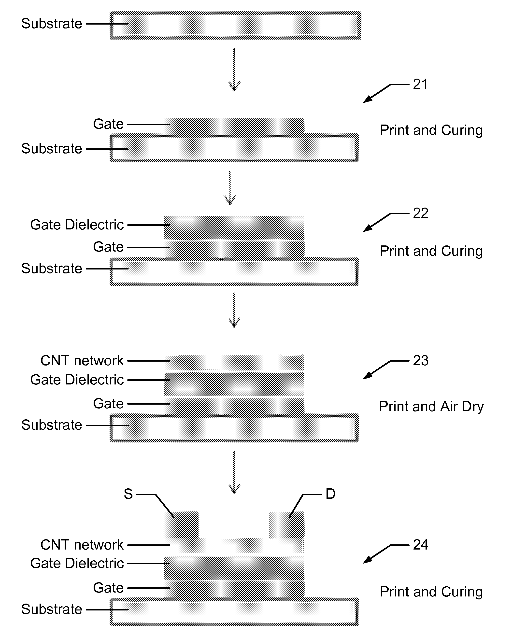
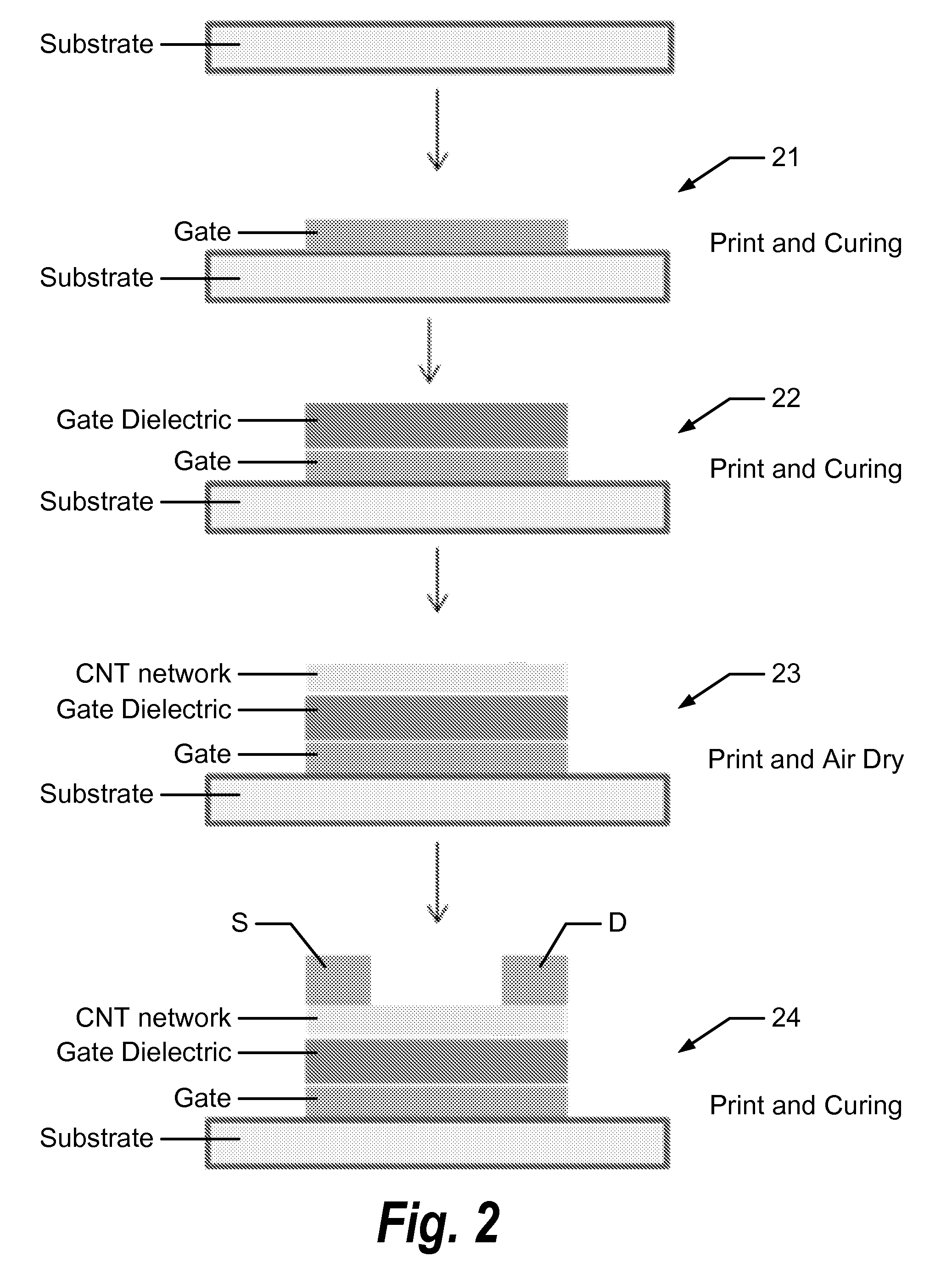
[0026]One or more embodiments of the invention are described below. It should be noted that these and any other embodiments are exemplary and are intended to be illustrative of the invention rather than limiting. While the invention is widely applicable to different types of systems, it is impossible to include all of the possible embodiments and contexts of the invention in this disclosure. Upon reading this disclosure, many alternative embodiments of the present invention will be apparent to persons of ordinary skill in the art.

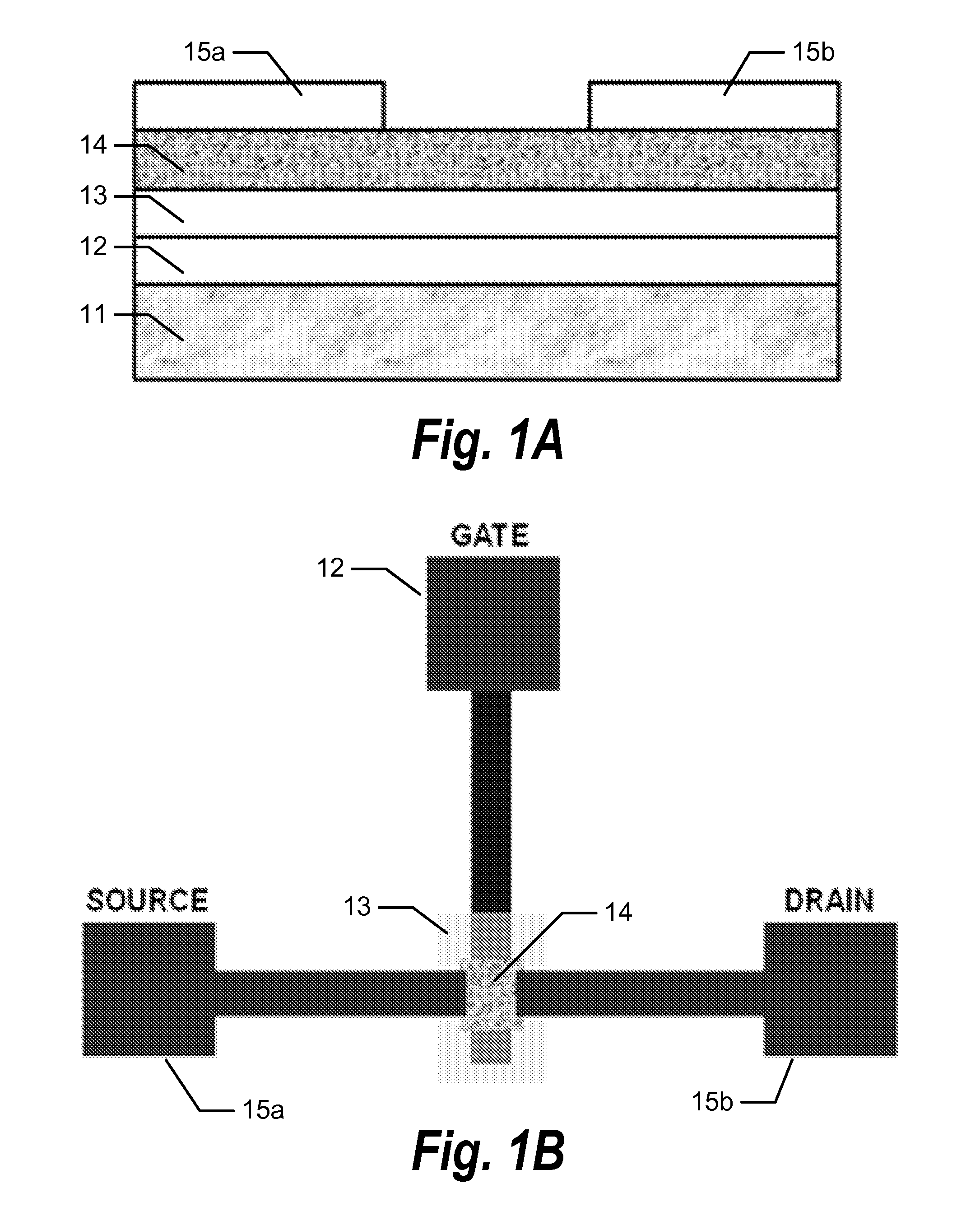
[0027]The present invention is directed to an apparatus and method of printable carbon nanotube (CNT) field effect transistors (FET).

[0028]While most of the terms used herein will be recognizable to those of skill in the art, the following definitions are nevertheless put forth to aid in understanding of the present invention.

[0029]“Nanotube,” as defined herein, refers to any tube with nanoscale dimensions.

[0030]“Carbon nanotube,” as defined herein, refers ...


PUM


Abstract

Methods and devices for manufacturing carbon nanotube based field effect transistors are disclosed including providing a substrate; printing a gate electrode layer onto the substrate and sintering and / or UV curing; printing a gate isolation layer onto the gate electrode and air drying and / or UV curing; printing one or more carbon nanotube channel layers onto the gate isolation layer, wherein each carbon nanotube channel layer is air dried prior to subsequent printings; and printing a source and drain electrode layer onto the one or more carbon nanotube channel layers and sintering and / or UV curing. Other embodiments are described and claimed.

Description

STATEMENT REGARDING FEDERALLY SPONSORED RESEARCH[0001]The U.S. Government has a paid-up license in this invention and the right in limited circumstances to require the patent owner to license others on reasonable terms as provided for by the terms of the contract NNX09CA37C awarded by NASA.BACKGROUND OF THE INVENTION[0002]1. Field of the Invention[0003]This invention relates generally to the field of printed flexible or rigid electronics, and more specifically to methods and devices for the manufacture of carbon nanotube based field effect transistors (CNT-FETs).[0004]2. Background of the Invention[0005]Carbon nanotubes (CNT) have many unique electrical and mechanical properties. CNT based transistors are being investigated by many research groups (Tan et al., Nature, 1998 (393), Martel et al., Appl. Phys. Lett. 1998 (73), Rogers et al., RSC Chemistry World, 2008 July). Many devices are based on a single CNT as a channel placed between source and drain electrodes. These kinds of dev...

Claims


Application Information

Patent Timeline
Patent Type & Authority Applications(United States)
IPC IPC(8): H01L51/10H01L51/30H01L51/40
CPCB82Y10/00H01L51/0005H01L51/0022H01L51/0048H01L51/0541H01L51/0558H01L51/0545H10K71/135H10K71/611H10K85/221H10K10/464H10K10/484H10K10/466H10K50/16
Inventor CHEN, YIHONGCHEN, RAY T.
Owner OMEGA OPTICS
Why Eureka
Try Eureka