
Combined Write Assist and Retain-Till-Accessed Memory Array Bias

a memory array and write assist technology, applied in static storage, information storage, digital storage, etc., can solve the problems of increasing the dc data retention current drawn by the embedded memory array, the power consumption of the electronic circuitry in those devices and systems is of great concern, and the array bias is reduced. , to achieve the effect of reducing the array bias

Active Publication Date: 2011-10-27
TEXAS INSTR INC
View PDF1 Cites 10 Cited by
  • Summary
  • Abstract
  • Description
  • Claims
  • Application Information

AI Technical Summary

Benefits of technology

[0026]Embodiments of this invention provide a static random access memory (SRAM) in which features of write assist power supply bias and a reduced array bias in a retain-till-accessed (RTA) are efficiently provided to the SRAM arrays.
[0027]Embodiments of this invention provide such an SRAM in which write assist power consumption is reduced relative to conventional write assist circuitry, by way of a self-regulating mechanism.
[0028]Embodiments of this invention provide such an SRAM in which write disturb errors in adjacent unselected columns sharing a sense amplifier with the selected column are avoided.
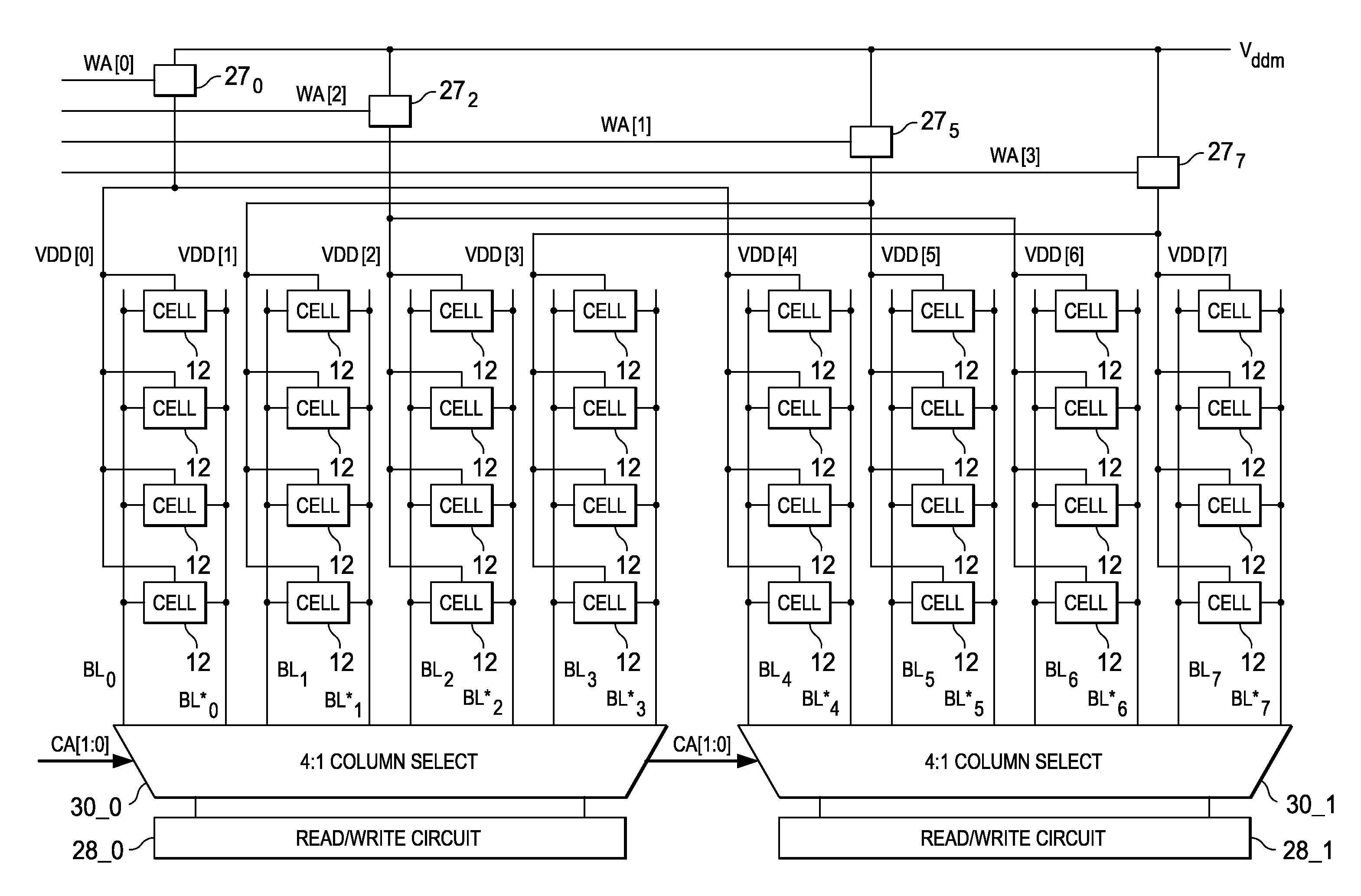
[0030]Embodiments of this invention can be realized by constructing a static random access memory (SRAM) array in which a bias device is series-connected between a power supply voltage and the load transistors in each memory cell of a given column of the array, with a switching transistor in parallel with that bias device for each column. The memory array can be constructed in multiple memory array blocks. In operation, the switching transistors short out corresponding bias devices during read operations, and at other times in which the memory array block is to be fully powered. In RTA mode for the memory array block, all switching devices for that memory array block are turned off, allowing the bias device to the SRAM cells to be defined by the voltage drop across the corresponding bias devices. In write cycles, the switching devices for selected columns are turned off, allowing the reduced power supply voltage to bias the selected cells in those columns. The switching devices for unselected columns can be turned on, providing full power supply bias to unselected columns and reducing the likelihood of write disturb errors in shared sense amplifier architectures.

Problems solved by technology

The power consumption of the electronic circuitry in those devices and systems is therefore of great concern, as battery life is often a significant factor in the buying decision as well as in the utility of the device or system.
However, this physical scaling of device sizes raises significant issues in connection with such embedded memory.
One such problem is the substantial DC current due to sub-threshold leakage and other short channel effects of the transistors in SRAM cells, resulting in increased DC data retention current drawn by embedded memory arrays.
However, significant recovery time is typically involved in biasing the memory array to an operational state from the retention state.
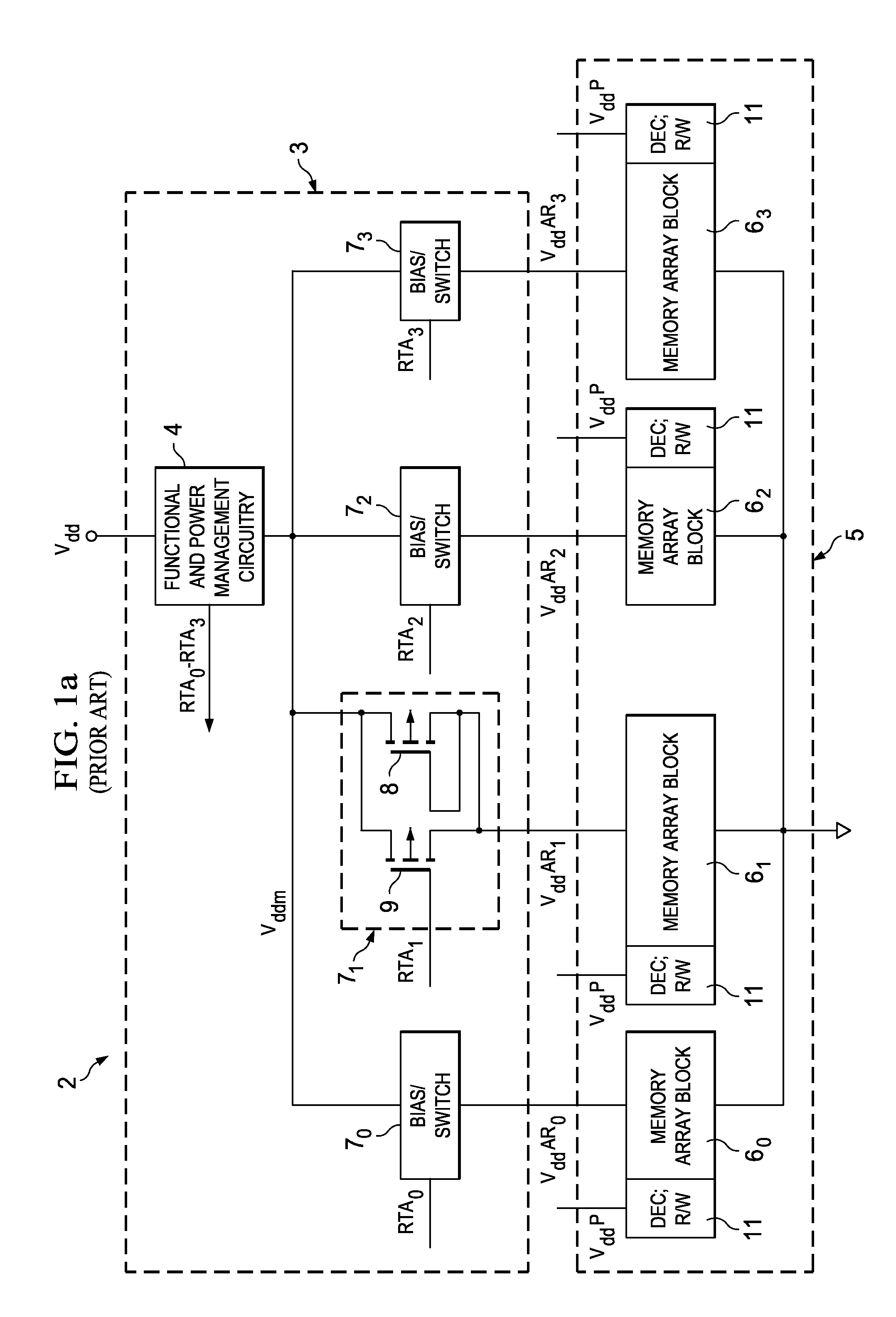
Because of its ability to be applied to individual blocks within a larger-scale integrated circuit, as well as its fast recovery time, the RTA standby mode is now often used with embedded memories in modern mobile Internet devices and smartphones, considering that these devices remain powered-on but not fully active for much of their useful life.
As mentioned above, if transistors 13, 14 are extremely small sub-micron devices, these leakage currents can be significant (as much as 1 nA per memory cell), and can thus result in significant overall standby power consumption if the number of memory cells 12 in memory array blocks 6 is large.
A second problem encountered in connection with embedded SRAM memory now realized by modern manufacturing technology stems from the increased variability in the electrical characteristics of transistors formed at these extremely small feature sizes.
This variability in characteristics has been observed to increase the likelihood of read and write functional failures, on a cell-to-cell basis.
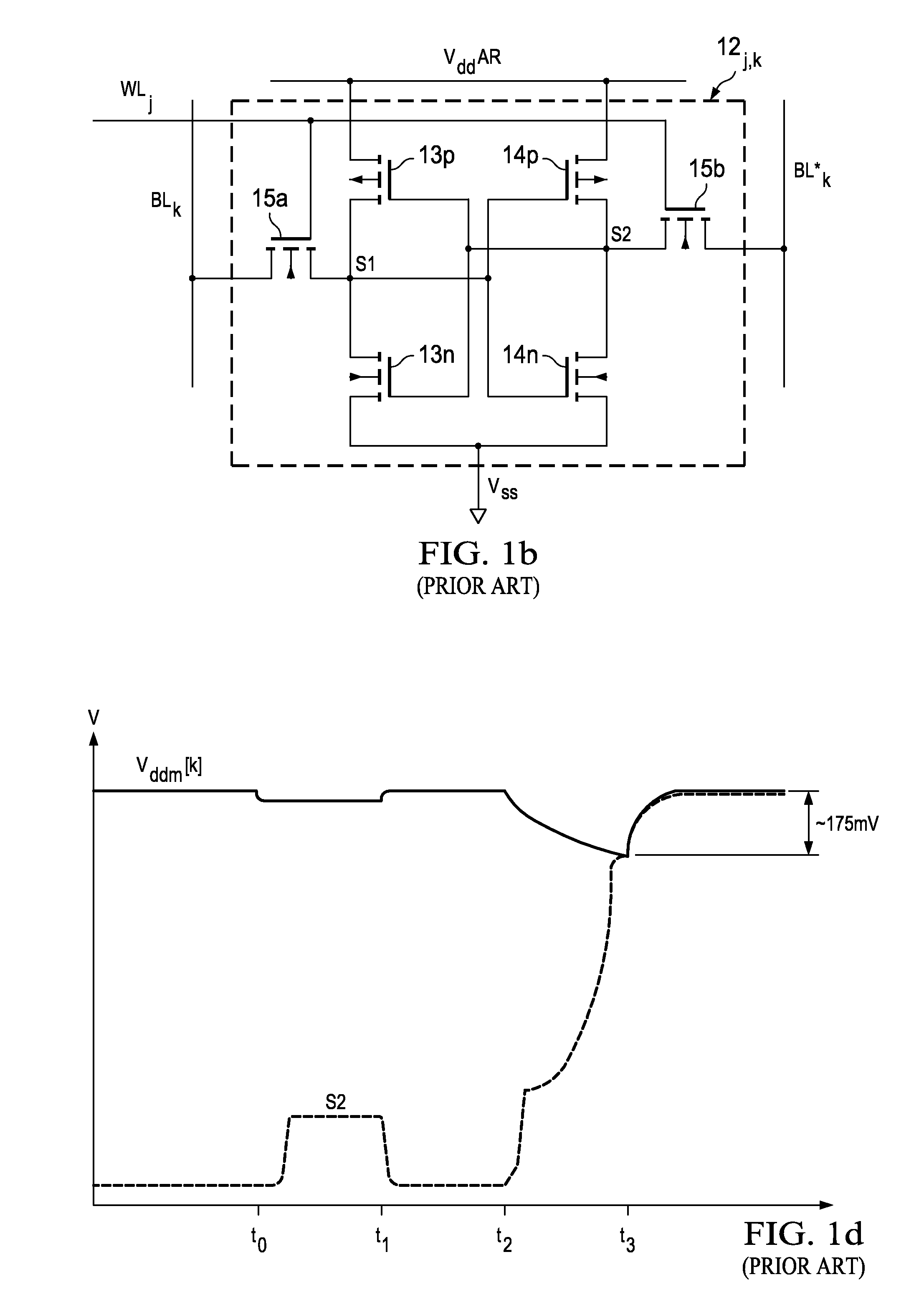
A particular failure mode that has been observed in conventional modern SRAM memories is the failure to switch the state of an SRAM cell in a write operation.
Typically, this failure has been observed to be due to the inability of write circuitry to pull down the sense node currently latched to a high voltage.
The write has failed.
While this conventional write assist approach allows a weak cell to be written, as described above, it has been observed that this approach involves substantial power consumption.

Method used


Image

  • Combined Write Assist and Retain-Till-Accessed Memory Array Bias
  • Combined Write Assist and Retain-Till-Accessed Memory Array Bias
  • Combined Write Assist and Retain-Till-Accessed Memory Array Bias

Examples


Embodiment Construction

[0043]The present invention will be described in connection with its preferred embodiment, namely as implemented into an integrated circuit including an embedded memory array, and constructed according to complementary metal-oxide-semiconductor (CMOS) technology. However, it is contemplated that the benefits of this invention may be attained when realized in other applications and constructed according to other technologies. Accordingly, it is to be understood that the following description is provided by way of example only, and is not intended to limit the true scope of this invention as claimed.

[0044]Referring now to FIG. 2a, by way of example, integrated circuit 20 constructed according to embodiments of this invention will now be described at a block diagram level. As shown in FIG. 2, integrated circuit 20 includes functional circuitry 23, power management circuitry 24, and memory array blocks 26. The functionality provided by functional circuitry 23 may vary widely depending o...


PUM


Abstract

Bias circuitry for a static random-access memory (SRAM) with a retain-till-accessed (RTA) mode and with write assist bias in a normal operating mode. The memory is constructed of multiple memory array blocks of SRAM cells. Bias devices are associated with each memory array block, and associated with one or more columns. Each bias device includes a diode-connected transistor in parallel with a shorting transistor, between a power supply voltage and a power supply bias node for cells in its column or columns. The shorting transistor receives control signals from control logic so that the diode-connected transistor for each column is shorted during read cycles, and in write cycles in which its columns are not selected; in write cycles in which its columns are selected, the shorting transistor in the bias device is turned off, so that a reduced power supply voltage is applied to the selected column. The shorting transistors for all columns in the block are turned off in the RTA mode. An additional transistor in series with the diode-connected transistor may be included, to enable a floating power supply bias mode.

Description

CROSS-REFERENCE TO RELATED APPLICATIONS[0001]This application is related to commonly assigned U.S. patent application Ser. No. 12 / ______, entitled “Reduced Power Consumption in Retain-Till-Accessed Static Memories” and Ser. No. 12 / ______, entitled “Retain-Till-Accessed Power Saving Mode in High Performance Static Memories”, both filed contemporaneously herewith and incorporated herein by reference.STATEMENT REGARDING FEDERALLY SPONSORED RESEARCH OR DEVELOPMENT[0002]Not applicable.BACKGROUND OF THE INVENTION[0003]This invention is in the field of integrated circuits. Embodiments of this invention are more specifically directed to solid-state static random access memories (SRAMs), and power reduction in those SRAMs.[0004]Many modern electronic devices and systems now include substantial computational capability for controlling and managing a wide range of functions and useful applications. Many of these electronic devices and systems are now handheld portable devices. For example, man...

Claims


Application Information

Patent Timeline
IPC IPC(8): G11C7/00
CPCG11C11/413
Inventor CLINTON, MICHAEL PATRICKHOLLA, LAKSHMIKANTHA V.MENEZES, VINOD
Owner TEXAS INSTR INC
Learn More