Electrostatic discharge protection having multiply segmented diodes in proximity to transistor

a diode and electrostatic discharge technology, applied in the direction of emergency protective circuit arrangement, transistor, etc., can solve the problems of insufficient substrate pump effect, inability to rely on protection devices to achieve uniform trigger, and inability to achieve uniform trigger

Inactive Publication Date: 2011-11-03
TEXAS INSTR INC
View PDF1 Cites 21 Cited by
  • Summary
  • Abstract
  • Description
  • Claims
  • Application Information

AI Technical Summary

Benefits of technology

[0010]Applicants recognized that the ESD trigger currents It2 of protection devices in advanced semiconductor products of the wireless, RF, fail-safe, USB, IEC, and related families becomes unacceptably small, mostly because of the small size of these products and the relentless trend towards more scaling. In addition, applicants found that the protection devices cannot be relied upon for achieving uniform trigger and thus efficient protection, when the layouts of diode and transistor are done in random fashion; while the layout goal of minimum capacitive loading remains unchanged, the multitude of different I / O functions requires different layout specifications to become compatible with the respective pin specification. In particular, it has to be avoided that in some layouts of the diode in relation to the transistor, only insufficient substrate pump effects are observed. Furthermore, applicants recognized that if a way could be found to increase the It2 density (A / μm) without initiating second breakdown, the same magnitude of It2 could be achieved with smaller consumption of semiconductor real estate.
[0012]Applicants solved the problem of increasing the trigger current It2 while keeping the diode area constant by splitting the diode area into two halves, then leaving one half area in its original location while positioning the hitherto under-utilized diode half area symmetrically on the opposite side of the nMOS transistor. In this new position, the second, hitherto under-utilized diode half area carries its full share of the SCR portion of It2, thus balancing the trigger current flow, while simultaneously participating fully as an additional heat sink. The resistance of the trigger current is reduced, allowing higher It2 values without a need for increasing the total diode area and a risk of thermal runaway. While achieving this, the net capacitance is conserved.
[0013]Applicants further found that an additional increase of It2 is obtained when the distances between the two n-wells of the diode halves and the transistor diffusions are reduced to the closest proximity free of electrical shorts. By reducing the distances, the contribution of the semiconductor substrate to the electrical resistance of the bipolar trigger current portion can be reduced, allowing more current before heating and thermal runaway.
[0015]It is a technical advantage that the concept of dividing the diode area can be extended to applications, where the still finer slices of diode area are placed on three or four sides of the MOS transistor. It is another technical advantage that the concept can be applied to drain-extended MOS transistors.
[0016]It is a further technical advantage that the concept of the invention is applicable to I / Cs in p-type semiconductor bulk conductivity and thus to protection devices with nMOS transistors, as well as to I / Cs in n-type bulk conductivity and thus to protection devices with pMOS transistors.

Problems solved by technology

Applicants recognized that the ESD trigger currents It2 of protection devices in advanced semiconductor products of the wireless, RF, fail-safe, USB, IEC, and related families becomes unacceptably small, mostly because of the small size of these products and the relentless trend towards more scaling.
In addition, applicants found that the protection devices cannot be relied upon for achieving uniform trigger and thus efficient protection, when the layouts of diode and transistor are done in random fashion; while the layout goal of minimum capacitive loading remains unchanged, the multitude of different I / O functions requires different layout specifications to become compatible with the respective pin specification.
In particular, it has to be avoided that in some layouts of the diode in relation to the transistor, only insufficient substrate pump effects are observed.

Method used


Image

  • Electrostatic discharge protection having multiply segmented diodes in proximity to transistor
  • Electrostatic discharge protection having multiply segmented diodes in proximity to transistor
  • Electrostatic discharge protection having multiply segmented diodes in proximity to transistor

Examples


Embodiment Construction

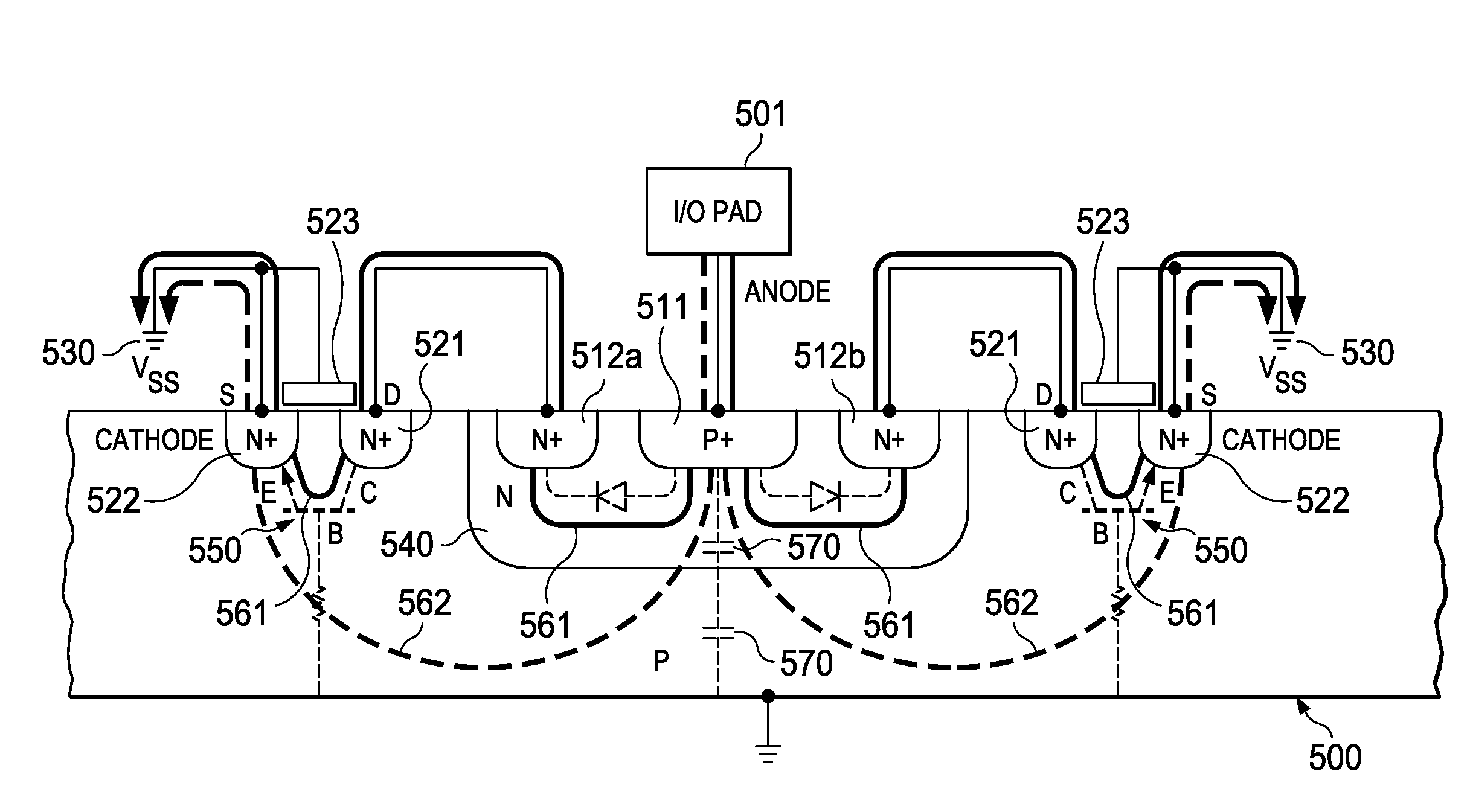
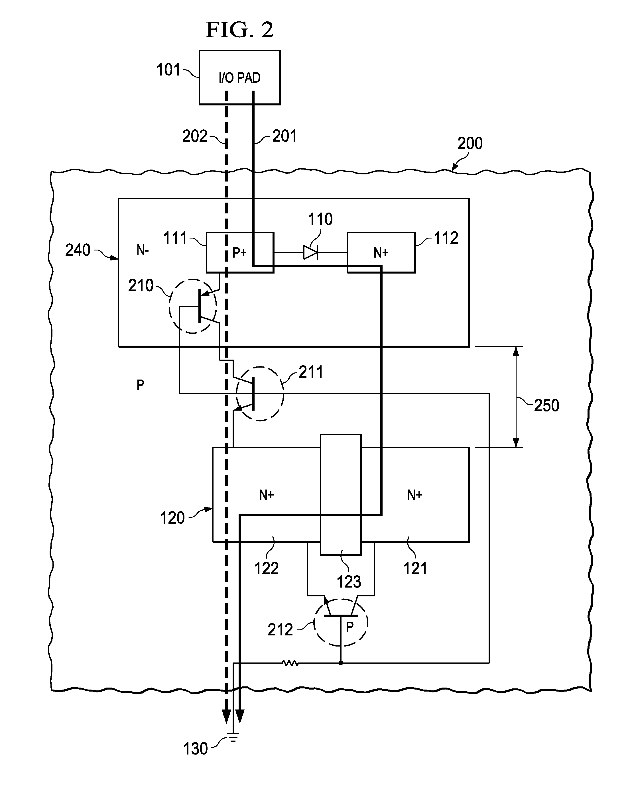
[0023]FIG. 1 shows the block diagram of the concept referred to as the diode isolated grounded-gate MOS concept for protecting fail-safe, RF, wireless, and other advanced ICs in a semiconductor device against ESD events. The input / output (I / O) pad 101 to be protected is in series with the forward biased diode 110 and MOS transistor 120 to ground potential 130. Pad 101 is connected with the anode 111 of diode 110; the cathode 112 of the diode is tied to the drain 121 of MOS transistor 120.

[0024]The integrated circuit (I / C) and the device for ESD protection are fabricated in a semiconductor substrate. The term “substrate” refers herein to the starting semiconductor wafer, which, in present manufacturing, typically has p-type doping. For clarity, this case is also selected as the basis for the following discussions. For many applications, the first conductivity type referenced above is p-type and the opposite conductivity type is n-type. With this selection, the semiconductor substrate...


PUM


Abstract

An ESD protection device for an I / O pad (401); the device comprising a MOS transistor (420) having at least one elongated source region (422) and at least one elongated drain region (421) in a substrate (400) of first conductivity, the length (420a) of the source and drain regions oriented in a direction, the source tied to ground potential (430); a diode having an area including at least one elongated anode region and at least one elongated cathode region in a well of opposite conductivity, the lengths of the anode and cathode regions oriented in the same direction as the transistor regions; the diode area and the well divided normal to the lengths of the anode and cathode regions into two portions (anode portions 411x, 411y, cathode portions 412x, 412y, length portions 410x, 410y, well portions 440x, 440y); and the anode portions connected to the I / O pad, and the cathode portions connected to the transistor drain.

Description

FIELD OF THE INVENTION[0001]The present invention is related in general to the field of semiconductor devices and processes, and more specifically to the structure, layout, and fabrication method of low capacitance electrostatic discharge protection devices having multiply segmented diodes in close proximity to, and on two or more sides of transistors.DESCRIPTION OF RELATED ART[0002]Integrated circuits (ICs) may be severely damaged by electrostatic discharge (ESD) events. A major source of ESD exposure to ICs is from the human body (described by the “Human Body Model”, HBM); the discharge of the human body generates peak currents of several amperes to the IC for about 100 ns. A second source of ESD is from metallic objects (described by the “Machine model”, MM); it can generate transients with significantly higher rise times and current levels than the HBM ESD source. A third source is described by the “charged device model” (CDM), in which the IC itself becomes charged and discharg...

Claims


Application Information

Patent Timeline
Patent Type & Authority Applications(United States)
IPC IPC(8): H01L27/06H01L21/8234
CPCH01L27/0207H01L27/0629H01L27/0262
Inventor DUVVURY, CHARVAKALIN, YEN-YI
Owner TEXAS INSTR INC
Why Eureka
Try Eureka