

Electrochromic devices
- Summary
- Abstract
- Description
- Claims
- Application Information
AI Technical Summary
Benefits of technology
Problems solved by technology
Method used
Image

Examples
examples
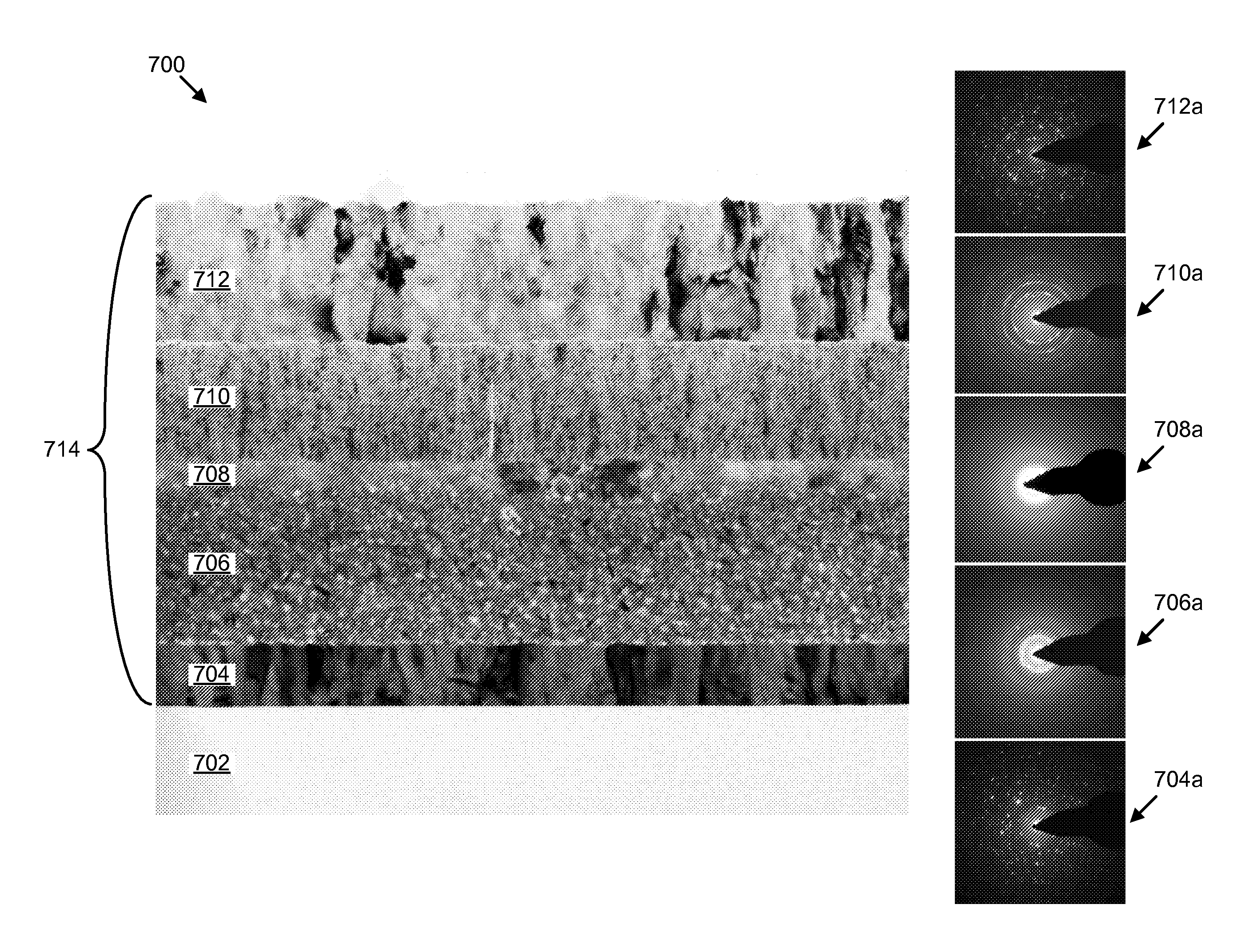
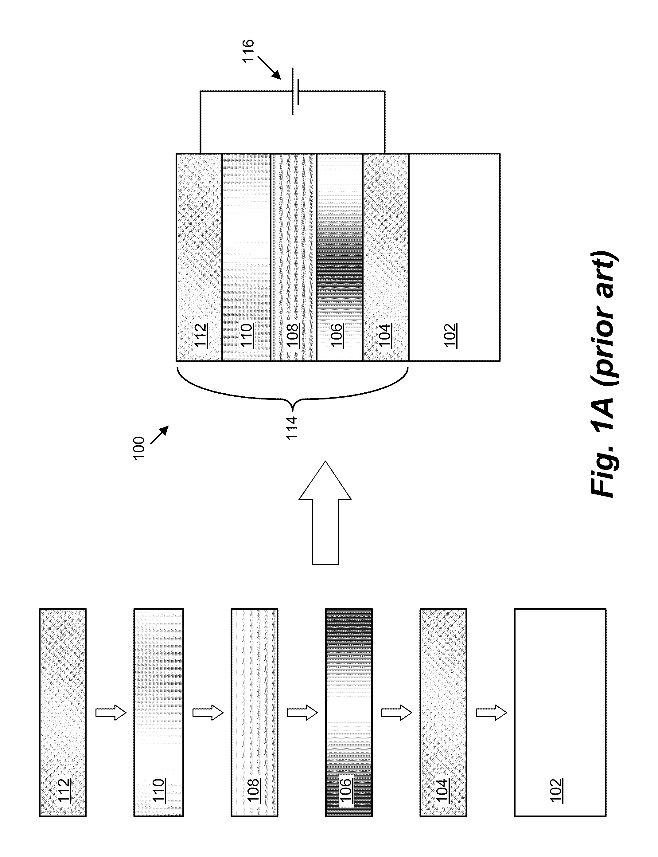
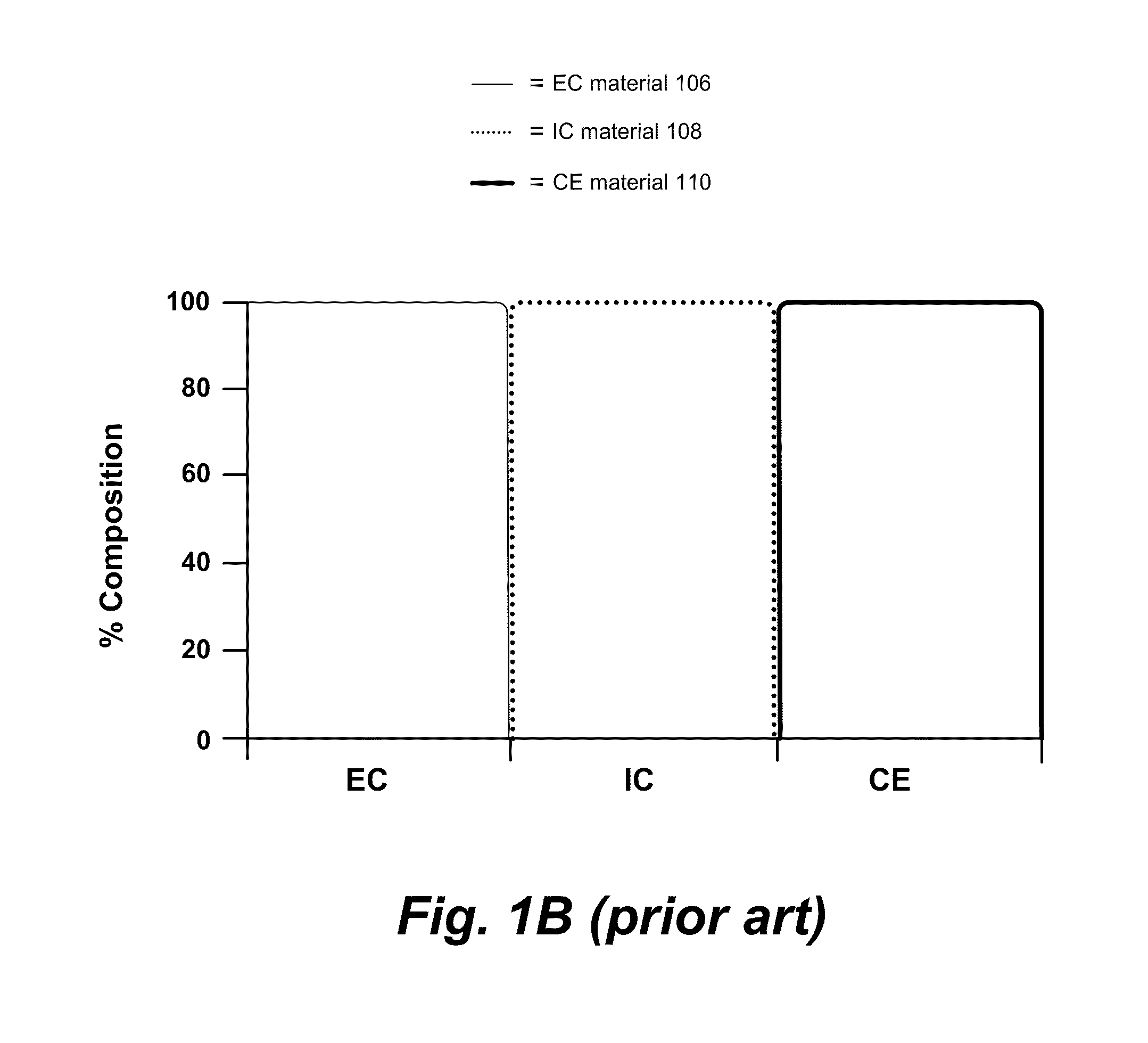
[0112]FIG. 6, is a graph of a process flow used as a protocol for fabricating electrochromic devices of the invention. They axis units are optical density and the x axis units are time / process flow. In this example, an electrochromic device is fabricated analogous to that described in relation to FIG. 4A, where the substrate is glass with fluorinated tin oxide as the first TCO, the EC layer is WO3 with excess oxygen in the matrix (for example, sputtered using the tungsten target, where the sputter gas is about 60% O2 and about 40% Ar), the CE layer is formed atop the EC layer and is made of NiWO and the second TCO is indium tin oxide (ITO). Lithium is used as the ion source for the electrochromic transition.
[0113]Optical density is used to determine endpoints during fabrication of the electrochromic device. Starting at the origin of the graph, optical density is measured as the EC layer, WO3, is deposited on the substrate (glass+TCO). The optical density of the glass substrate has a...
PUM
| Property | Measurement | Unit |
|---|---|---|
| Temperature | aaaaa | aaaaa |
| Temperature | aaaaa | aaaaa |
| Temperature | aaaaa | aaaaa |
Abstract
Description
Claims
Application Information