LED structure

a technology of light-emitting diodes and led sheets, which is applied in the direction of semiconductor/solid-state device manufacturing, electrical equipment, semiconductors, etc., can solve the problems of difficult to maintain the balance between light-permeability and current distribution uniformity, and difficult to achieve stable films. the effect of light-permeability and sheet resistance reduction

Active Publication Date: 2011-11-10
NAT CENT UNIV +1
View PDF4 Cites 21 Cited by
  • Summary
  • Abstract
  • Description
  • Claims
  • Application Information

AI Technical Summary

Benefits of technology

[0008]One objective of the present invention is to provide an LED structure to e

Problems solved by technology

However, the nickel-gold alloy and the chromium-gold alloy have inferior light permeability.
Nevertheless, a stable film is hard to be attained if the thickness thereof is too thin.
Therefore, it is difficult to keep the balance between light permeability and current distribution uniformity.
Although the TCO film has 90% light permeability and above, the ohmic contact between the TCO film and the

Method used


Image

  • LED structure
  • LED structure
  • LED structure

Examples


Embodiment Construction

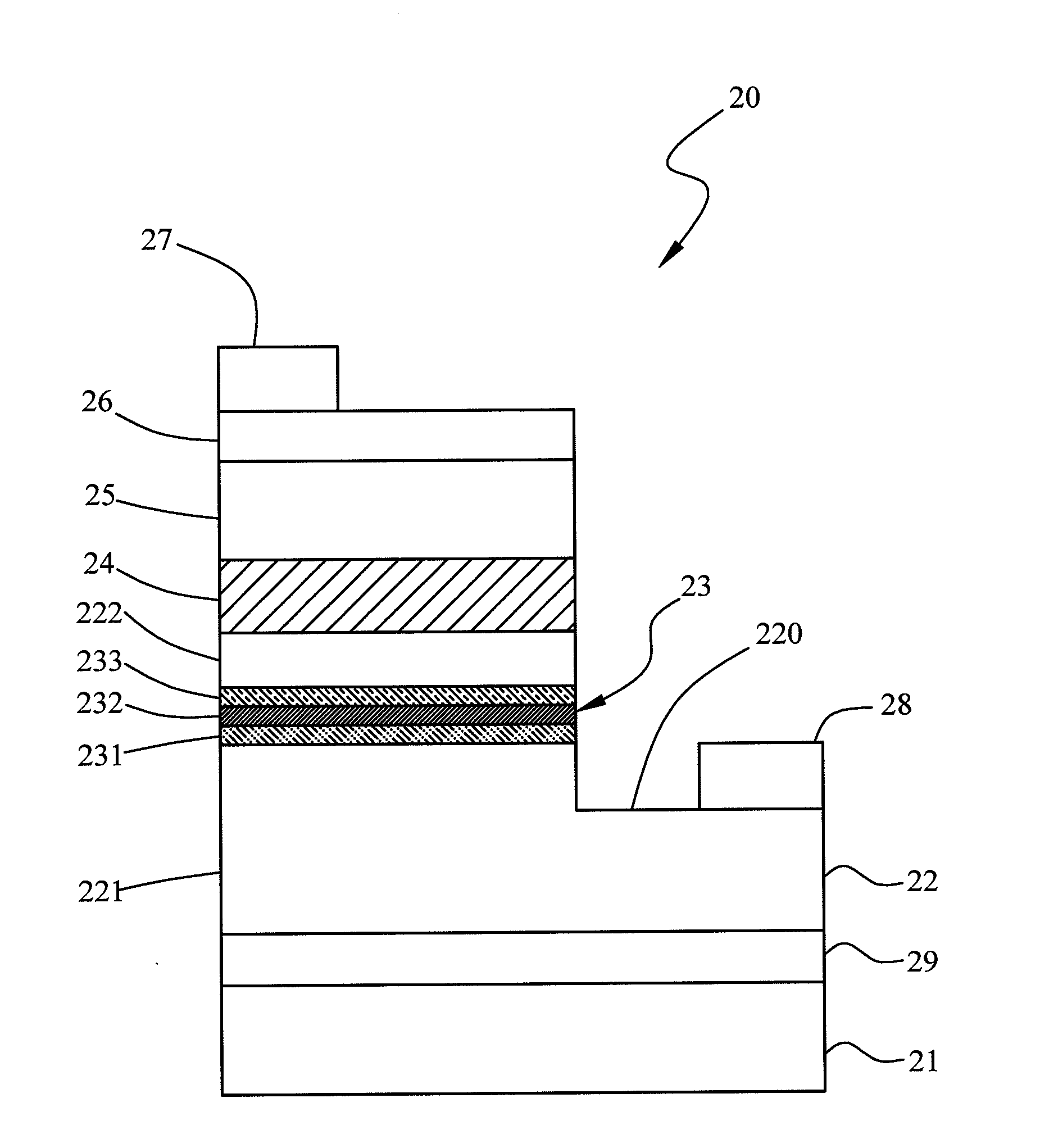
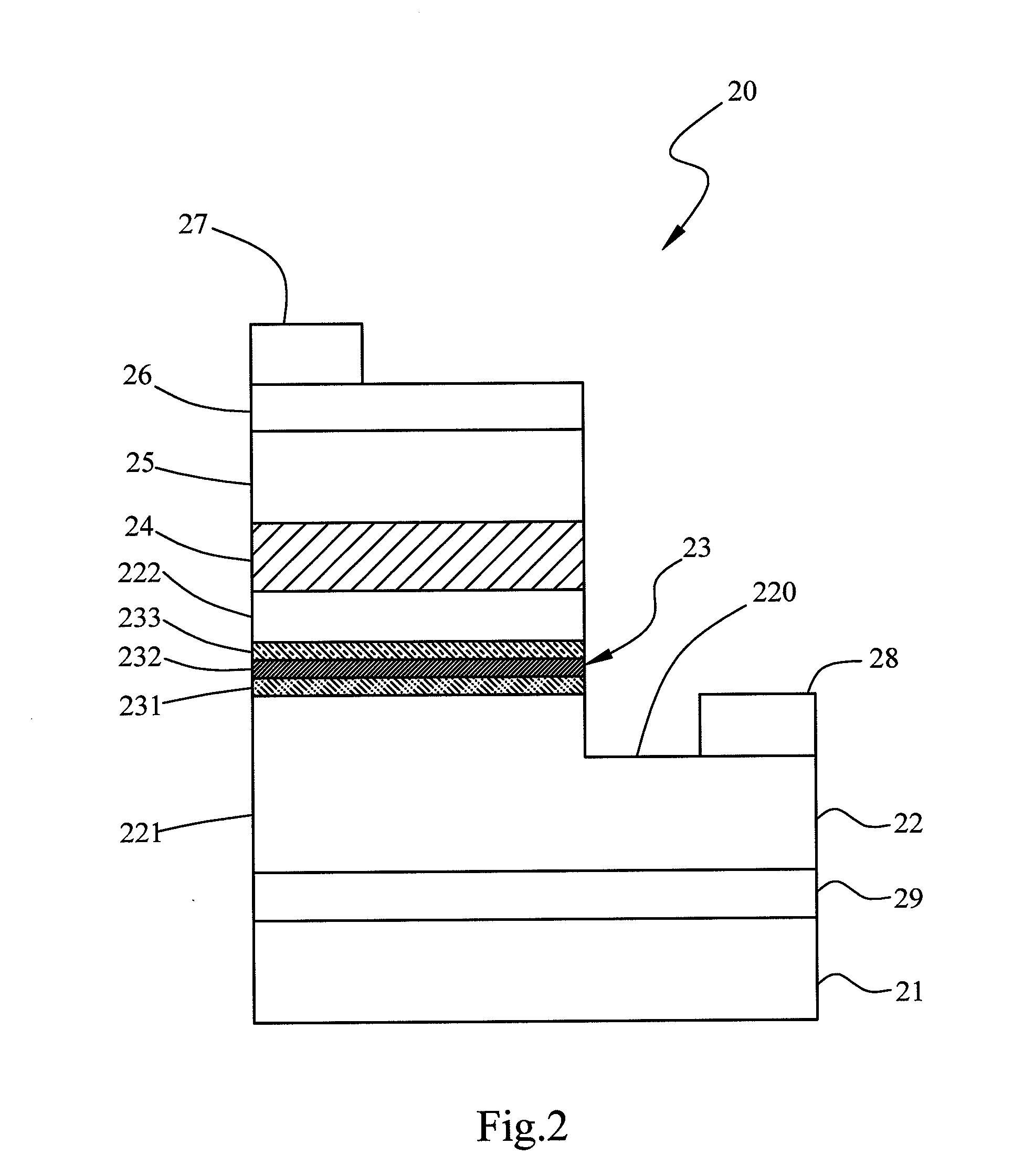
[0018]The present invention provides at least one N-type current spreading layer between the N-type semiconductor layers to uniformly distribute current in the lateral sides of the N-type semiconductor layers, whereby the N-type semiconductor layers have a higher electron concentration and lower sheet resistance. Here, it should be explained that the “P-type” or “N-type” in the P-type and N-type current spreading layers does not mean the current spreading layer is doped with P-type or N-type atoms but is referred to the current spreading layer is arranged in a P-type or N-type region. The materials used by the current spreading layer of the present invention will be further described thereinafter. The technical contents of the present invention will be demonstrated in accompany with the drawings below.

[0019]Refer to FIG. 2 a diagram schematically showing an LED structure according to one embodiment of the present invention. The LED structure 20 of the present invention comprises a s...


PUM


Abstract

The present invention discloses an LED structure, wherein an N-type current spreading layer is interposed between N-type semiconductor layers to uniformly distribute current flowing through the N-type semiconductor layer. The N-type current spreading layer includes at least three sub-layers stacked in a sequence of from a lower band gap to a higher band gap, wherein the sub-layer having the lower band gap is near the substrate, and the sub-layer having the higher band gap is near the light emitting layer. Each sub-layer of the N-type current spreading layer is expressed by a general formula InxAlyGa(1-x-y)N, wherein 0≦x≦1, 0≦y≦1, and 0≦x+y≦1.

Description

FIELD OF THE INVENTION[0001]The present invention relates to an LED (Light Emitting Diode) structure, particularly to an LED structure able to improve current distribution.BACKGROUND OF THE INVENTION[0002]LED (Light Emitting Diode) has advantages of compactness, longer lifespan, superior color performance, lower power consumption, and higher light emitting efficiency. Under the trend of environmental protection, LED has massively replaced the conventional lighting sources. Since an important breakthrough of gallium nitride LED was made in 1993 in Japan, gallium nitride LED has become a hot field of research around the world.[0003]Refer to FIG. 1 for a conventional LED structure. The conventional LED structure 10 comprises a substrate 11, an N-type semiconductor layer 12, a light emitting layer (or called the active layer) 13, a P-type semiconductor layer 14, a P-type current spreading layer 15, a first electrode 16 and a second electrode 17. The N-type semiconductor layer 12 is form...

Claims


Application Information

Patent Timeline
IPC IPC(8): H01L33/32
CPCH01L33/14H01L33/04
Inventor CHEN, PENG-RENLIU, HSUEH-HSINGCHYI, JEN-INN
Owner NAT CENT UNIV
Why Eureka
Try Eureka