Semiconductor apparatus and power supply circuit

a technology of power supply circuit and semiconductor, applied in the direction of transformer/inductance details, semiconductor devices, semiconductor/solid-state device details, etc., can solve the problems of reducing the efficiency of dc-dc converter, oscillation of output voltage, unstabilized operation, etc., to achieve excellent heat dissipation, stable operation, and small and thin

Inactive Publication Date: 2011-11-24
HITACHI METALS LTD
View PDF6 Cites 21 Cited by
  • Summary
  • Abstract
  • Description
  • Claims
  • Application Information

AI Technical Summary

Benefits of technology

[0009]Accordingly, an object of the present invention is to provide a stably operable semiconductor apparatus with excellent heat dissipation, which

Problems solved by technology

However, because the integrated semiconductor circuit device 106 is connected to lower surface pads through via-holes 110 in the laminate 150, the via-holes 110 generate parasitic inductance, reducing the efficiency of the DC-DC converter and causing the oscillation of output voltage, resulting in the unstabilized operation.
Also, because the integrated semiconductor circuit device 106 is packaged, it is more expensive than a bare-chip type.
Further, this DC-DC converter is poor in the heat dissipation

Method used


Image

  • Semiconductor apparatus and power supply circuit
  • Semiconductor apparatus and power supply circuit
  • Semiconductor apparatus and power supply circuit

Examples


example 1

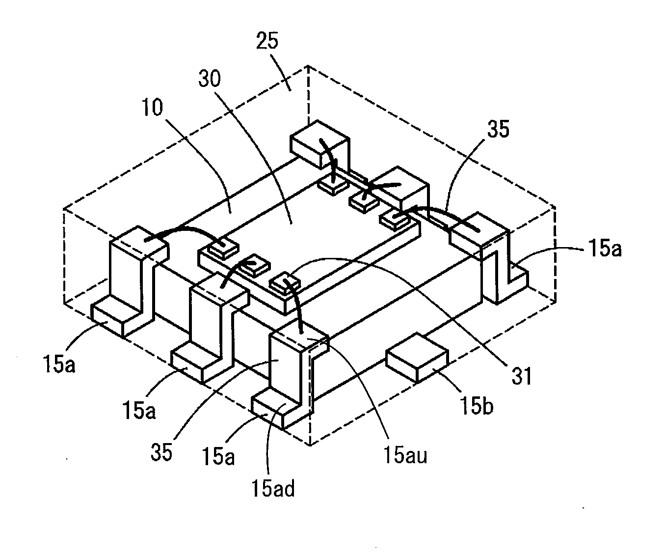
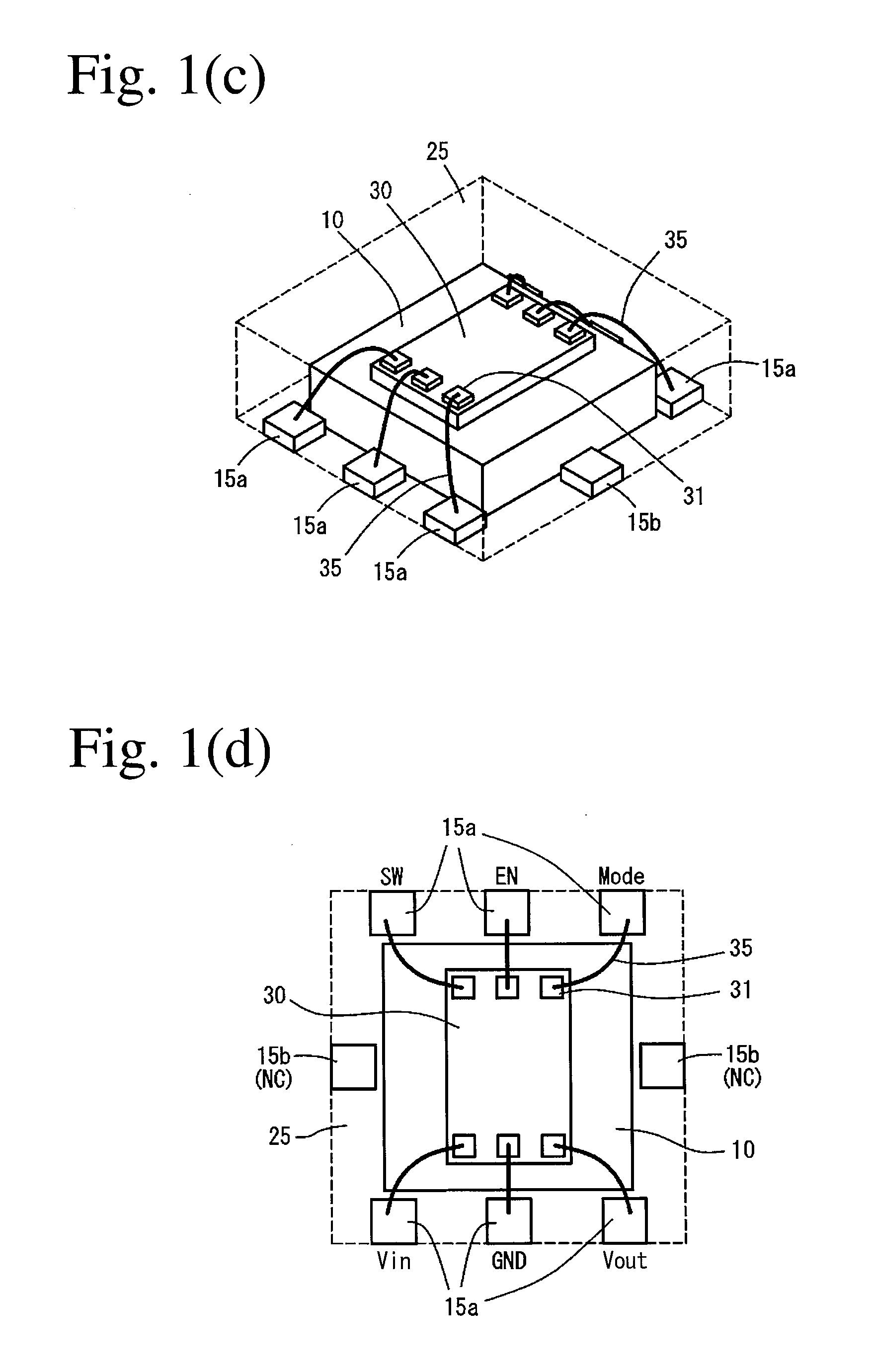
[0067]FIG. 11 shows one example of methods for producing the semiconductor apparatus of the present invention having the structure shown in FIGS. 1(a)-1(d). To assemble the semiconductor apparatus, the leadframe 50 shown in FIG. 2 was used. The leadframe 50 was produced by etching a 0.15-mm-thick copper alloy sheet and plating it with Ag. To improve solderability, the leadframe 50 was provided with Sn—Bi plating on the rear surface.

[0068]The leadframe 50 comprises pluralities of tie bars 52 perpendicularly extending inside the frame 51, to divide the inside of the frame 51 to pluralities of (15 in this Example) compartments each for forming a semiconductor apparatus. In each compartment, leads 55a, 55b extend integrally from the frame 51 and the tie bars 52, and a free end of each lead 55a, 55b does not reach a center of each compartment to define an opening 56. The leads 55a, 55b extend linearly with the same width and length, but they may have different width and length. Also, eac...

example 2

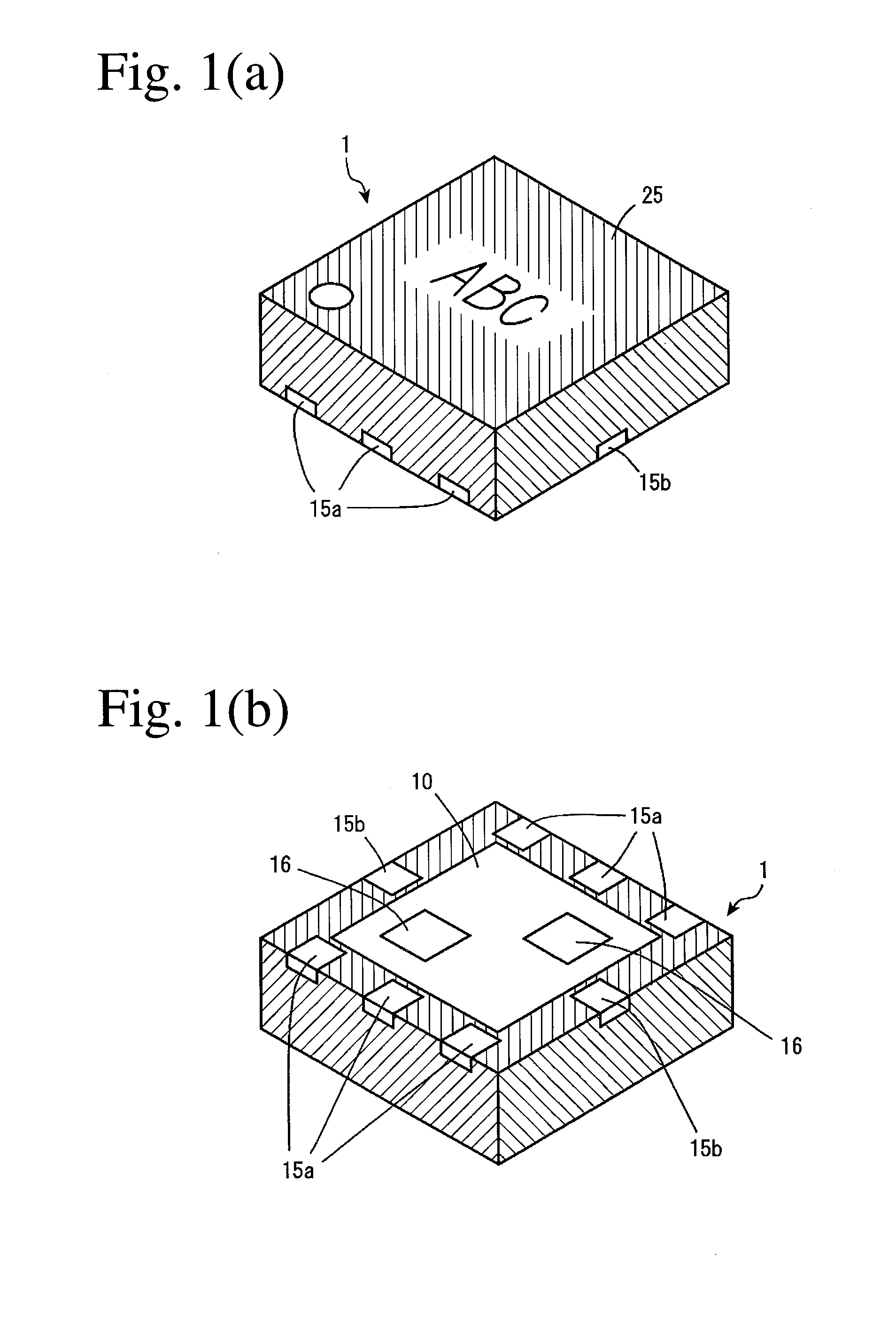
[0077]The semiconductor apparatus shown in FIGS. 13(a)-13(c) and having an outer size of 2.1 mm×2.1 mm×0.9 mm was produced in the same manner as in Example 1, except for using a leadframe 50 free of leads 55b acting as terminals NC. Because the inductor 10 has a larger mounting region by the absence of the terminals NC, the inductor 10 used may be larger in a planar direction than that of Example 1. Because of the expanded magnetic path area, a thinner inductor may be used than in Example 1 as long as it has the same inductance. Because the inductor 10 used in this Example had an outer size of 2.1 mm×1.5 mm×0.45 mm, two opposing sides of the inductor 10 were exposed from the molding resin 25. This semiconductor apparatus was thinner than that of Example 1 by the thickness of the inductor 10 despite no difference in electric characteristics. The inductor 10 and the integrated semiconductor circuit device 30 were not cracked even in the three-point bending test.


PUM


Abstract

A semiconductor apparatus comprising an integrated semiconductor circuit device having pluralities of electrode pads, pluralities of first external terminals connected to the electrode pads of the integrated semiconductor circuit device, an inductor disposed in a region surrounded by the first external terminals, and a resin portion sealing them, the integrated semiconductor circuit device being arranged on an upper surface of the inductor, and the inductor being exposed from a lower surface of the resin portion together with the first external terminals.

Description

FIELD OF THE INVENTION[0001]The present invention relates to a semiconductor apparatus in which an integrated semiconductor circuit device comprising switching transistors and a control circuit and an inductor are resin-sealed, particularly to a semiconductor apparatus constituting a DC-DC converter, and a power supply circuit comprising such a semiconductor apparatus.BACKGROUND OF THE INVENTION[0002]Various portable electronic apparatuses (cell phones, personal digital assistants PDA, note-type personal computers, DVD players, CD players, digital cameras, digital video cameras, etc.) comprise secondary batteries such as lithium ion batteries as power supplies. Because lithium ion batteries usually generate voltage of about 3.6 V (3.0 V to 4.2 V), electronic apparatuses comprise step-down or step-up DC-DC converters for obtaining operation voltage. The DC-DC converters are used in charging circuits, too.[0003]A DC-DC converter generally has a structure comprising an integrated semic...

Claims


Application Information

Patent Timeline
IPC IPC(8): H01L27/06
CPCH01L23/495H01L23/49531H01L2924/13091H01L2224/45147H01L2224/45144H01L2224/32225H01L2224/16225H01L2224/73204H01L2924/014H01L2924/01023H01L2924/01019H01L2924/01006H01L2924/01005H01L24/49H01L24/48H01L2924/30107H01L2924/19105H01L2924/19042H01L23/49822H01L23/50H01L24/97H01L2223/54406H01L2223/54486H01L2224/48091H01L2224/48247H01L2224/49171H01L2224/97H01L2924/01003H01L2924/01004H01L2924/01012H01L2924/01013H01L2924/01027H01L2924/01029H01L2924/01033H01L2924/01046H01L2924/01047H01L2924/01074H01L2924/01078H01L2924/01079H01L2924/01082H01L2924/01322H01L2924/09701H01L2924/14H01L2924/19041H01L2924/00014H01L2224/85H01L2924/00H01L24/45H01L2224/05554H01L2224/45014H01L2224/45139H01L2224/45169H01L2924/00011H01L2924/10161H01L2924/12042H01L2924/181H01L2224/05599H01L2924/00012H01L2224/45015H01L2924/207
Inventor UMENO, TOHRU
Owner HITACHI METALS LTD
Why Eureka
Try Eureka