Light Emitting Device

a technology of light emitting device and light source, which is applied in the direction of thermoelectric device junction materials, semiconductor devices, electrical apparatus, etc., can solve the problems of increasing the power consumption of light emitting devices, accelerating the deterioration of light emitting elements, and increasing the current supply of same amount of luminance, so as to achieve the effect of reducing the current flow between electrodes, increasing the luminance obtained when the same amount of current is supplied, and reducing the amount of current for

Inactive Publication Date: 2011-12-01
SEMICON ENERGY LAB CO LTD
View PDF8 Cites 53 Cited by
  • Summary
  • Abstract
  • Description
  • Claims
  • Application Information

AI Technical Summary

Benefits of technology

[0008]Further, luminous efficiency is different according to each luminescent color. To take a balance of luminance in whole emission of a light emitting device, it is required to apply a large amount of current for a light emitting element with inferior luminous efficiency; therefore, there is a disadvantage that deterioration of a light emitting element is accelerated.
[0019]According to the invention, luminance obtained when same amount of current is supplied can be increased compared with a light emitting element having a light emitting layer of a single layer. In other words, the amount of current for obtaining same luminance, which flows between electrodes, can be lowered.

Problems solved by technology

By increasing drive voltage, a problem of increasing power consumption of a light emitting device is led.
To take a balance of luminance in whole emission of a light emitting device, it is required to apply a large amount of current for a light emitting element with inferior luminous efficiency; therefore, there is a disadvantage that deterioration of a light emitting element is accelerated.

Method used


Image

  • Light Emitting Device
  • Light Emitting Device
  • Light Emitting Device

Examples


embodiment mode 1

[0041]In this embodiment mode, a structure of a light emitting element in which light emitting units are stacked is explained.

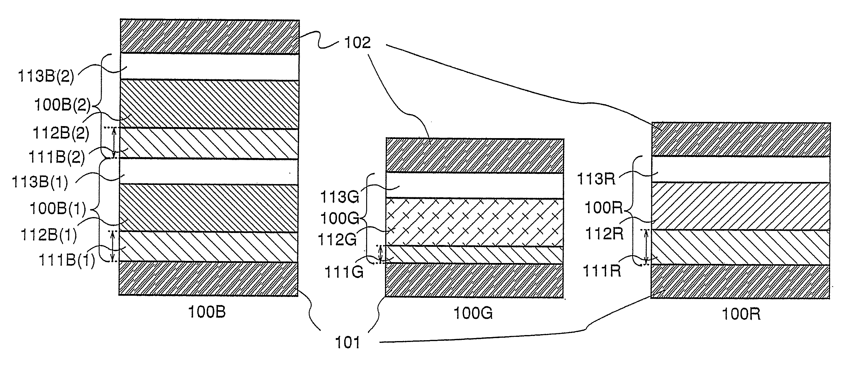
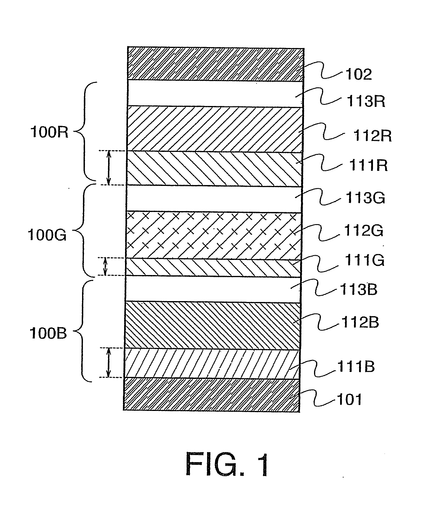
[0042]FIG. 1 shows a light emitting element in which a first light emitting unit 100B, a second light emitting unit 100G, and a third light emitting unit 100R are sequentially stacked between a first electrode 101 and a second electrode 102. The colors of light emitted from the light emitting units 100B, 100G, and 100R are not limited in particular. In this embodiment mode, however, a case where the first light emitting unit exhibits blue emission, the second light emitting unit exhibits green emission, and the third light emitting unit exhibits red emission is explained in this embodiment mode. The light emitting element in which light emitting units are stacked indicates a state where two or more light emitting units are stacked. In this embodiment mode, a state where three light emitting units are stacked is explained; however, the present invention is not...

embodiment mode 2

[0058]In this embodiment mode, a structure of a light emitting element which is different from that in the above-described embodiment mode is explained.

[0059]According to the present invention, a light emitting element in which light emitting units are stacked is not required to be applied to all light emitting elements formed over a substrate. A distance from each of light emitting layers to a first electrode 101 can be approximately oddly multiplied ¼ wavelength by controlling a thickness of a first layer 111 for at least one light emitting element, and accordingly, a state where luminous output efficiency is high can be obtained, luminous efficiency at the same current density can be enhanced, and density of current which is applied can be kept low. As a result of keeping current density low, the lifetime of the light emitting element can be improved. In this embodiment mode, a case where one light emitting element which exhibits one luminescent color is a light emitting element ...

embodiment mode 3

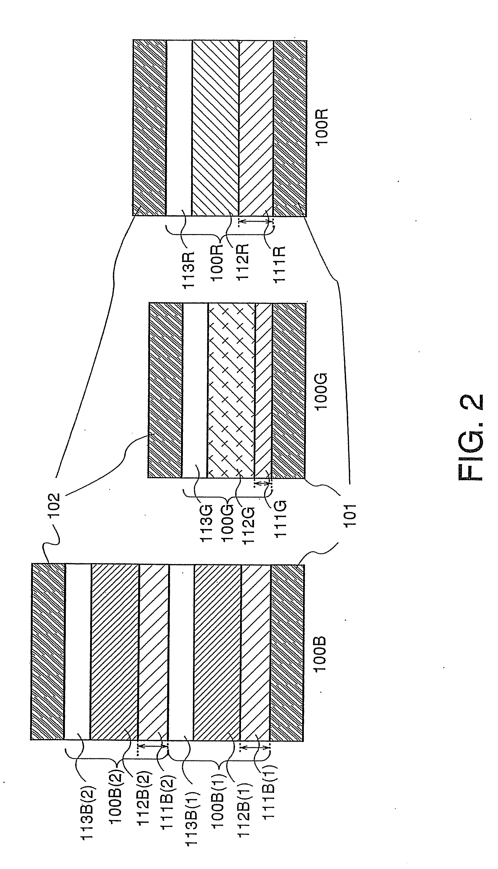
[0068]In this embodiment mode, a case where a stacked layer type light emitting element is applied to a light emitting element which exhibits different luminescent color from that in the above embodiment mode is explained.

[0069]In the present invention, a stacked layer type light emitting element may be used for an element except a first light emitting element 100B. For example, a single layer type light emitting element may be used as a light emitting element 100G which exhibits luminescent color with high sensitivity with respect to human eyes such as green emission, and accordingly, the light emitting element 100G may have a structure in which the number of light emitting layers included between a pair of electrodes is smaller than that of the stacked layer type light emitting elements 100R and 100B which exhibit red emission or blue emission, respectively.

[0070]The explanation of another structure is omitted since it is similar to the above embodiment mode.

[0071]In the stacked l...


PUM


Abstract

It is an object of the invention to provide a light emitting device which can display a superior image in which luminescent color from each light emitting layer is beautifully displayed and power consumption is lowered in a light emitting element in which light emitting layers are stacked. One feature of the invention is that, in a light emitting element which comprises light emitting layers stacked between electrodes, each distance between each light emitting layer and an electrode is approximately oddly multiplied ¼ wavelength by controlling a thickness of a layer provided therebetween to enhance luminous output efficiency. Another feature of the invention is that a drive voltage is lowered using a high conductive material for the layer compared with a conventional element.

Description

TECHNICAL FIELD[0001]The present invention relates to a light emitting device which can be utilized as a display means, a light source, or the like.BACKGROUND ART[0002]A display device including a light emitting element (hereinafter, referred to as a light emitting device) has a wider viewing angle and a higher response characteristic and operates with lower power consumption compared with a display device having a liquid crystal element, namely a liquid crystal display device. Therefore, the light emitting device has been actively developed.[0003]A light emitting element includes an organic material or an inorganic material between a pair of electrodes. By applying current to the organic material or inorganic material and exciting a light emitting material, a predetermined luminescent color can be obtained. To increase emission luminance of the light emitting element, a large amount of current may be supplied, in other words, high voltage may be applied to the pair of electrodes; t...

Claims


Application Information

Patent Timeline
Patent Type & Authority Applications(United States)
IPC IPC(8): H01L33/60H01L51/54
CPCH01L27/3211H01L27/3244H01L51/5218H01L51/5278H01L51/5044H01L51/5265H10K59/35H10K59/128H10K59/12H10K50/131H10K50/818H10K50/852H10K50/19H10K50/157H10K50/167
Inventor SEO, SATOSHINODA, TAKESHIYAMAZAKI, SHUNPEI
Owner SEMICON ENERGY LAB CO LTD
Why Eureka
Try Eureka