CMOS three-dimensional image sensor detectors with assured non collection of late arriving charge, more rapid collection of other charge, and with improved modulation contrast
a three-dimensional image sensor and detector technology, applied in the field of three-dimensional image sensor detectors, can solve the problems of shortened lifetime photocharges, degrade the accuracy and quality of presently acquired depth image data, and shorten the lifetime of photocharges, so as to maximize minimize the collection of photocharges, and maximize the collection of substantially all photocharges
- Summary
- Abstract
- Description
- Claims
- Application Information
AI Technical Summary
Benefits of technology
Problems solved by technology
Method used
Image

Examples
Embodiment Construction
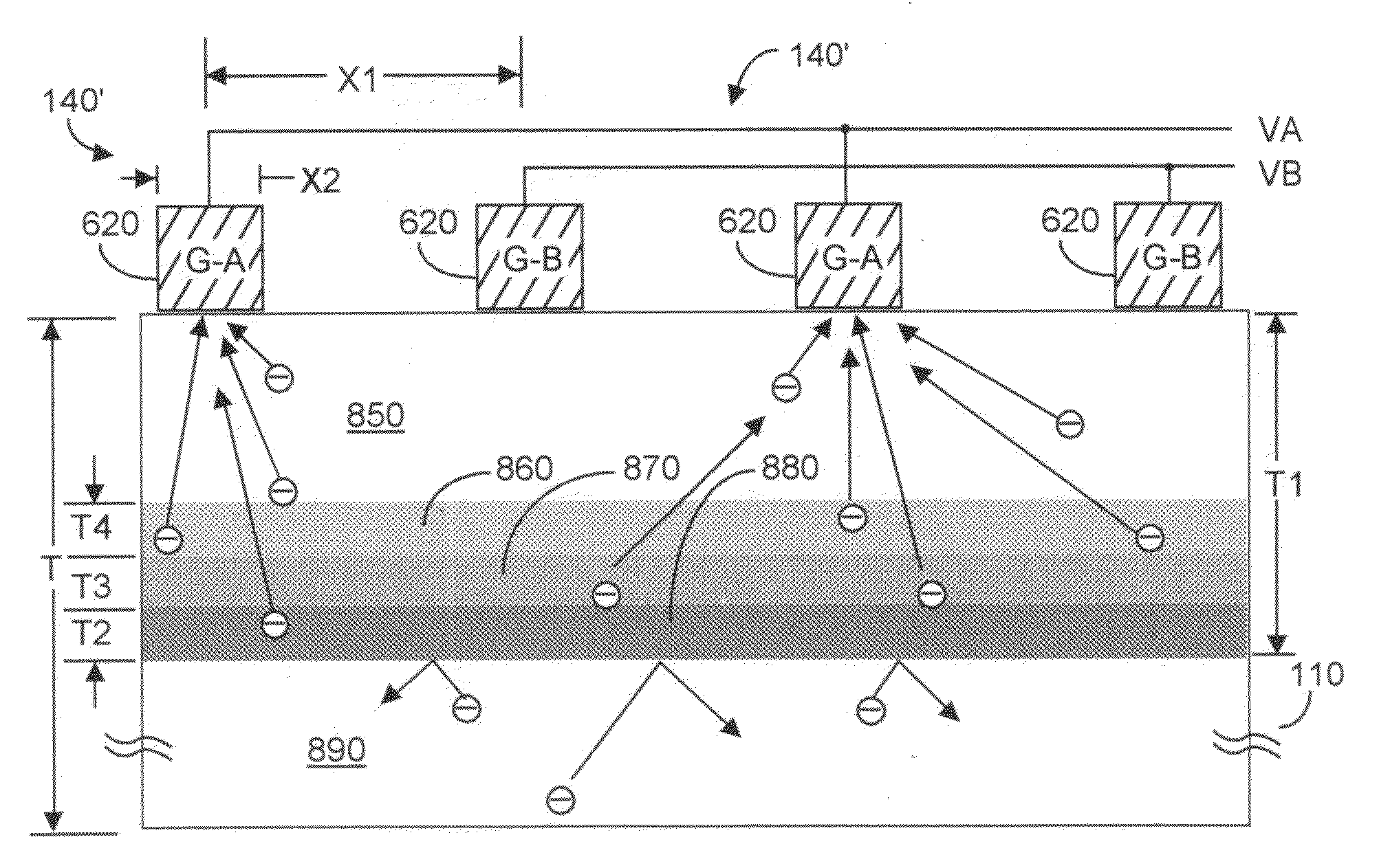
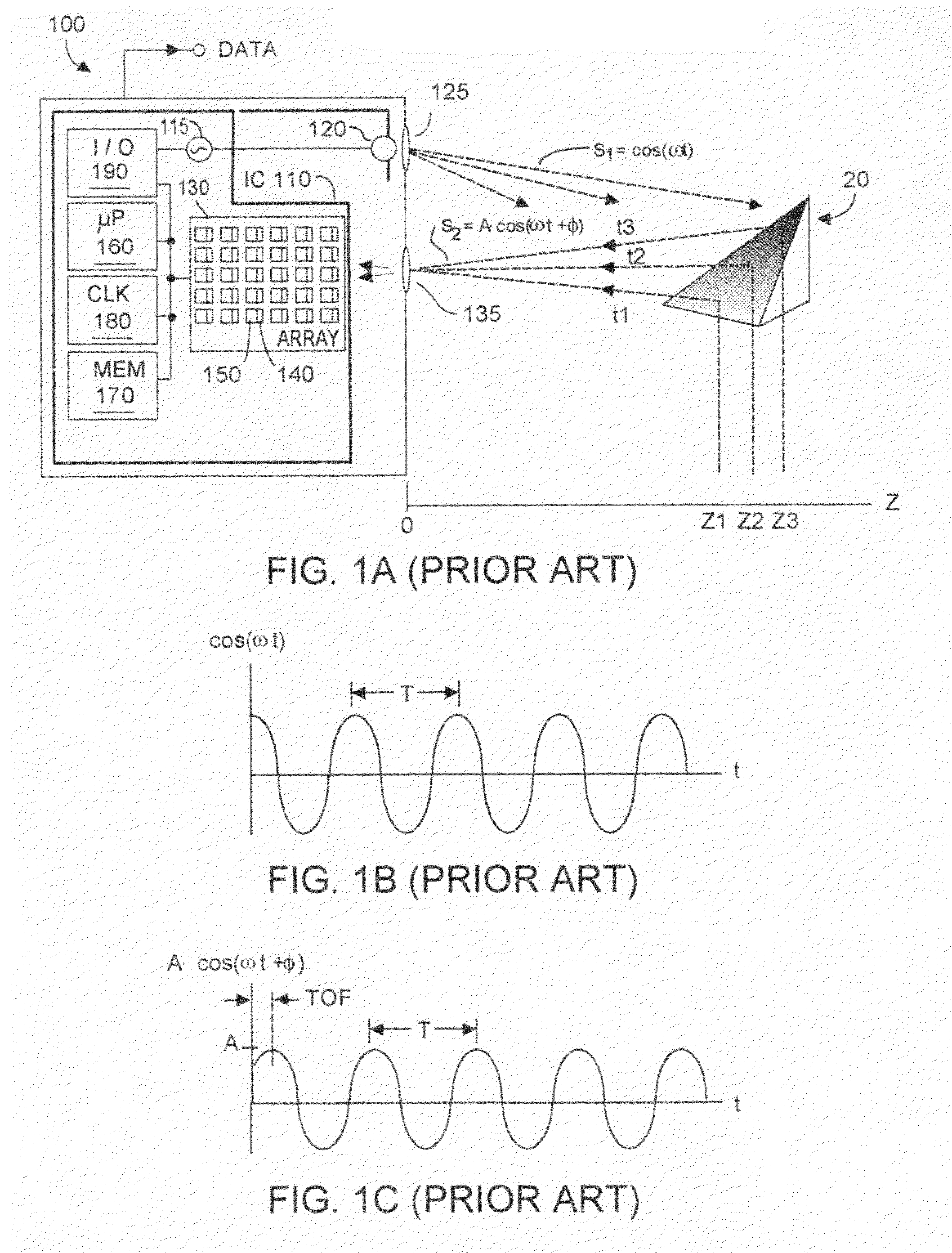
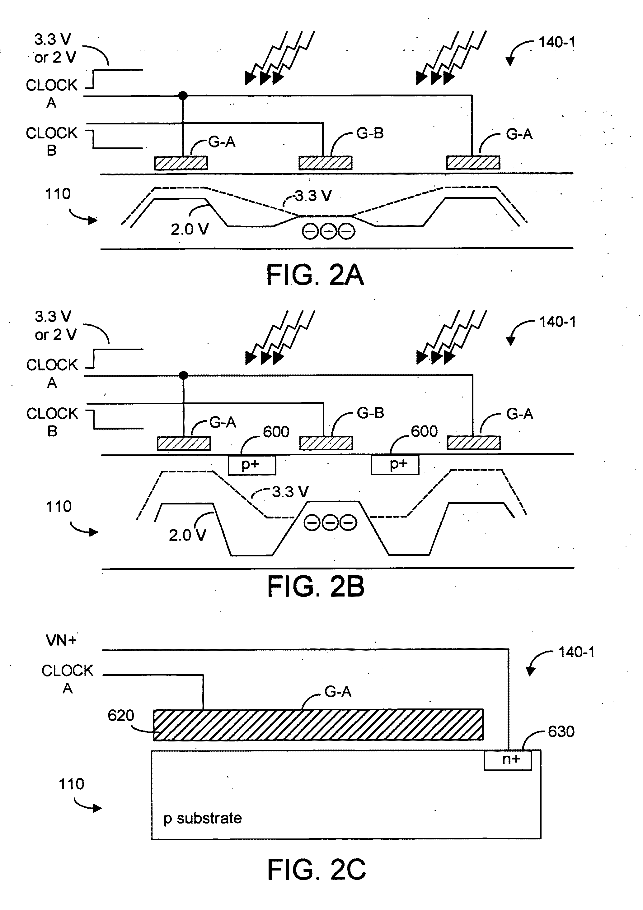
[0051]Embodiments of the present invention may be practiced with phase-based TOF systems such as depicted in FIG. 1A as exemplified by numerous U.S. patents to Canesta, Inc., including U.S. Pat. No. 7,352,454 (2008) or with non-phase based systems, e.g., as described in U.S. Pat. No. 6,323,942 (2001), assigned to Canesta, Inc. Embodiments of the present invention to improve collection of photocharge whose creation time is known, and to impede collection of photocharge whose creation time is not known (i.e., late arriving charge) can be implemented by modifying the structure of sensors 140 in FIG. 1A. Of course the present invention may be used with other sensors and may be used in non-TOF applications.
[0052]Sensors as described with respect to FIG. 1A, modeled on the '454 patent, thus are a good starting point. To recapitulate the description of the '454 sensors, the sensor structures included finger-shaped gate structures that extended along a y-axis, and were spaced-apart from eac...
PUM
 Abstract
Description
Claims
Application Information
PatSnap Eureka turns technology decisions into work you can execute. Powered by our Innovation Knowledge Graph, it runs expert workflows across engineering, life sciences, materials and intellectual property. Get your review-ready output in minutes.


