Wafer processing method, wafer polishing apparatus, and ingot slicing apparatus

Inactive Publication Date: 2011-12-01
DENSO CORP
View PDF7 Cites 7 Cited by
  • Summary
  • Abstract
  • Description
  • Claims
  • Application Information

AI Technical Summary

Benefits of technology

[0012]In view of the foregoing problems, it is an object of the present invention to provide a wafer processing method, a wafer polishing apparatus, and an ingot slicing apparatus that can improve a processing efficiency.
[0014]In the wafer processing method according to the first aspect, a reforming process for forming of the reformed layer and a polishing process for polishing the surface of the wafer can be performed as a parallel process or a single process. Thus, a wafer processing efficiency can be improved compared with a case where the reforming process and the polishing process are performed with different apparatuses. Furthermore, because the reformed layer is formed by applying the heat quantity, the wafer processing efficiency can be improved and a damage of a polishing apparatus can be restricted.
[0016]In the wafer processing method according to the second aspect, the reformed layer is formed by applying the heat quantity to a portion of the ingot and the ingot is sliced into the wafer by bringing the slicing tool into contact with the portion of the ingot applied with the heat quantity. Because the slicing tool cuts the reformed layer having a lower hardness than the ingot, a time required for slicing the ingot can be reduced compared with a case where the ingot is sliced without forming the reformed layer. Furthermore, because a surface roughness of the wafer can be restricted, a time required for planarizing the wafer can be reduced. Thus, a wafer processing efficiency can be improved.
[0018]The polishing apparatus according to the third aspect includes the polishing tool and the reforming unit. Thus, a wafer processing efficiency can be improved compared with a case where a reforming process for forming the reformed layer and a polishing process for polishing the wafer are performed with different apparatuses.
[0020]The slicing apparatus according to the fourth aspect includes the slicing tool and the reforming unit. Thus, the slicing apparatus can slice the ingot while applying the heat quantity to the portion of the ingot with which the slicing tool comes into contact and forming the reformed layer at the portion of the ingot. Because the slicing tool cuts the reformed layer having a lower hardness than the ingot, a time required for slicing the ingot can be reduced compared with a case where the ingot is sliced without forming the reformed layer. Furthermore, because a surface roughness of the wafer can be restricted, a time required for planarizing the wafer can be reduced. Thus, a wafer processing efficiency can be improved.

Problems solved by technology

Furthermore, because the reformed layer is formed by applying the heat quantity, the wafer processing efficiency can be improved and a damage of a polishing apparatus can be restricted.

Method used


Image

  • Wafer processing method, wafer polishing apparatus, and ingot slicing apparatus
  • Wafer processing method, wafer polishing apparatus, and ingot slicing apparatus
  • Wafer processing method, wafer polishing apparatus, and ingot slicing apparatus

Examples


first embodiment

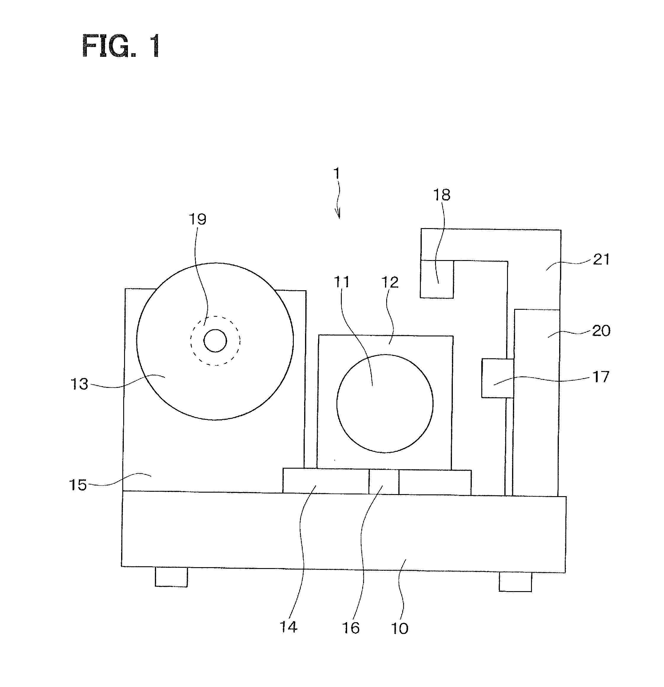
[0029]A slicing apparatus 1 according to a first embodiment will be described with reference to FIG. 1.

[0030]The slicing apparatus 1 includes a bed 10, an ingot holder 12, and a slicing tool 13. The bed 10 has a horizontal surface. The ingot holder 12 and the slicing tool 13 are disposed above the surface of the bed 10.

[0031]The ingot holder 12 is configured to hold an ingot 11 and includes a rotation mechanism which is not shown. The ingot holder 12 is disposed above the surface of the bed 10 through a saddle 14. The saddle 14 is expandable in a normal direction to the surface of the bed 10 and is movable in a parallel direction to the surface of the bed 10. Thus, by expanding and moving the saddle 14, the ingot holder 12 is movable in the normal direction to the surface of the bed 10 and the parallel direction to the surface of the bed 10. The ingot holder 12 holds the ingot 11 through the rotation mechanism. When a center axis of the ingot 11 extending in a longitudinal direction...

second embodiment

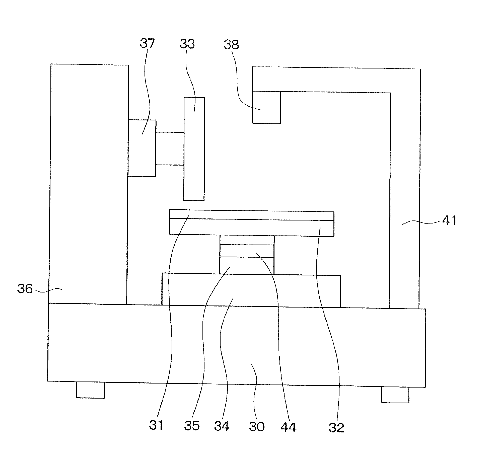
[0085]A slicing apparatus 1 and a polishing apparatus 3 according to a second embodiment will be described below. First, the slicing apparatus 1 will be described with reference to FIG. 5A and FIG. 5B

[0086]As shown in FIG. 5B, the slicing apparatus 1 includes the slicing tool 13 that includes a conductive bonding member 13a and a plurality of grindstones 13b arranged on a peripheral surface of the bonding member 13a. The slicing apparatus 1 further includes a power unit which is not shown. The power unit applies a predetermined voltage to the bonding member 13a and the ingot 11 so as to generate an arc discharge between the bonding member 13a and the ingot 11. The slicing apparatus 1 applies a heat quantity to the ingot 11 with the arc discharge and slices the ingot 11 with the grindstones 13b. Thus, the slicing tool 13 according to the present embodiment can function as a slicing tool for slicing the ingot 11 and can function as the reforming unit 17 for forming the reformed layer ...

third embodiment

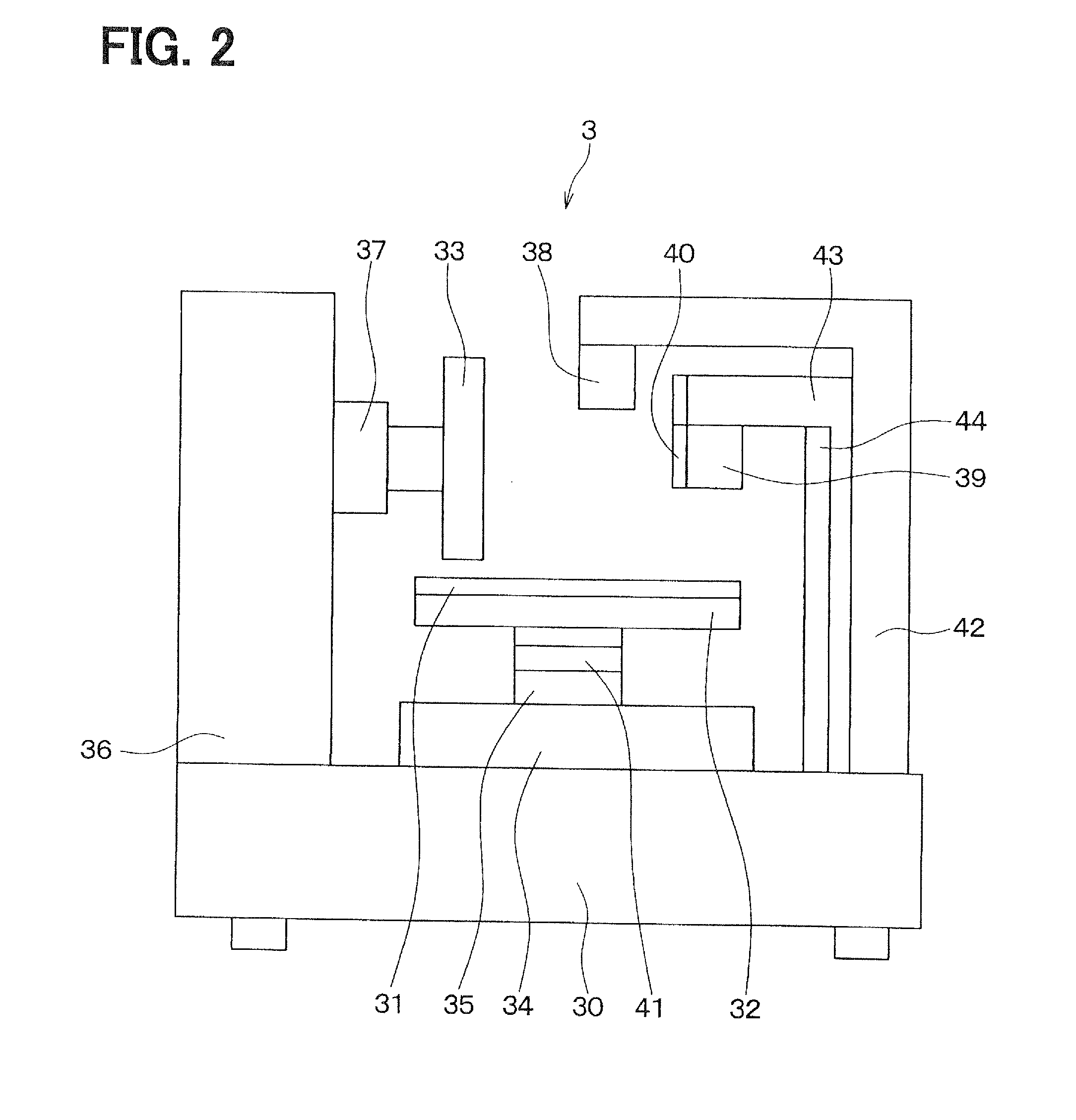
[0095]A polishing apparatus 3 according to a third embodiment will be described with reference to FIG. 7. The polishing apparatus 3 according to the present embodiment includes a reflective material applying unit in addition to the polishing apparatus 3 according to the first embodiment. The reflective material applying unit is not shown in FIG. 7.

[0096]In the polishing apparatus 3 according to the present embodiment, the wafer 31 is held by the wafer holder 32 in a state where the a reflective material 50 is applied to a surface of the wafer 31 so that protruding portions on the surface are exposed outside the reflective material 50. The reflective material 50 applied to the surface of the wafer 31 has a high reflective index. For example, the reflective material 50 is water having a reflective index of 1.33 or benzene having a reflective index of 1.428.

[0097]Thus, when the wafer 31 is polished with the polishing apparatus 3, first, the reflective material 50 is applied to the surf...


PUM

PropertyMeasurementUnit
Temperatureaaaaaaaaaa
Concentrationaaaaaaaaaa
Electrical resistanceaaaaaaaaaa

Abstract

In a wafer processing method, an ingot is sliced into a wafer and the wafer is planarized by polishing a surface of the wafer. When the wafer is planarized, the wafer is disposed on a wafer holder and the wafer is rotated, a heat quantity is applied to a portion of the wafer so as to form a reformed layer at the portion of the wafer, and a polishing tool is brought into contact with the portion of wafer while rotating so as to polish the portion of the wafer.

Description

CROSS REFERENCE TO RELATED APPLICATIONS[0001]The present application is based on and claims priority to Japanese Patent Application No. 2010-119204 filed on May 25, 2010, the contents of which are incorporated in their entirety herein by reference.BACKGROUND OF THE INVENTION[0002]1. Field of the Invention[0003]The present invention relates to a wafer processing method, a wafer polishing apparatus, and an ingot slicing apparatus.[0004]2. Description of the Related Art[0005]Conventionally, a wafer is formed by slicing an ingot and a wafer is planarized by polishing a surface of the wafer. In a case where a high hardness wafer such as a silicon carbide (SiC) wafer is planarized by polishing, a reformed layer having a lower harness than SiC is formed at a surface portion of the SiC wafer and the reformed layer is polished so as to improve a processing efficiently compared with a case where the SiC wafer is polished without forming a reformed layer.[0006]For example, JP-A-2009-283629 dis...

Claims


Application Information

Patent Timeline
IPC IPC(8): B24B1/00B28D1/02B24B49/16
CPCB28D5/0082H01L21/02013H01L21/02008B28D5/022
Inventor KOUTAKE, KYOHEIMORITA, HIROMICHIKANO, FUMIYOSHIYAMAGUCHI, TETSUJIINOMATA, SUMITOMONAGAYA, MASATAKE
Owner DENSO CORP
Why Eureka
Try Eureka