

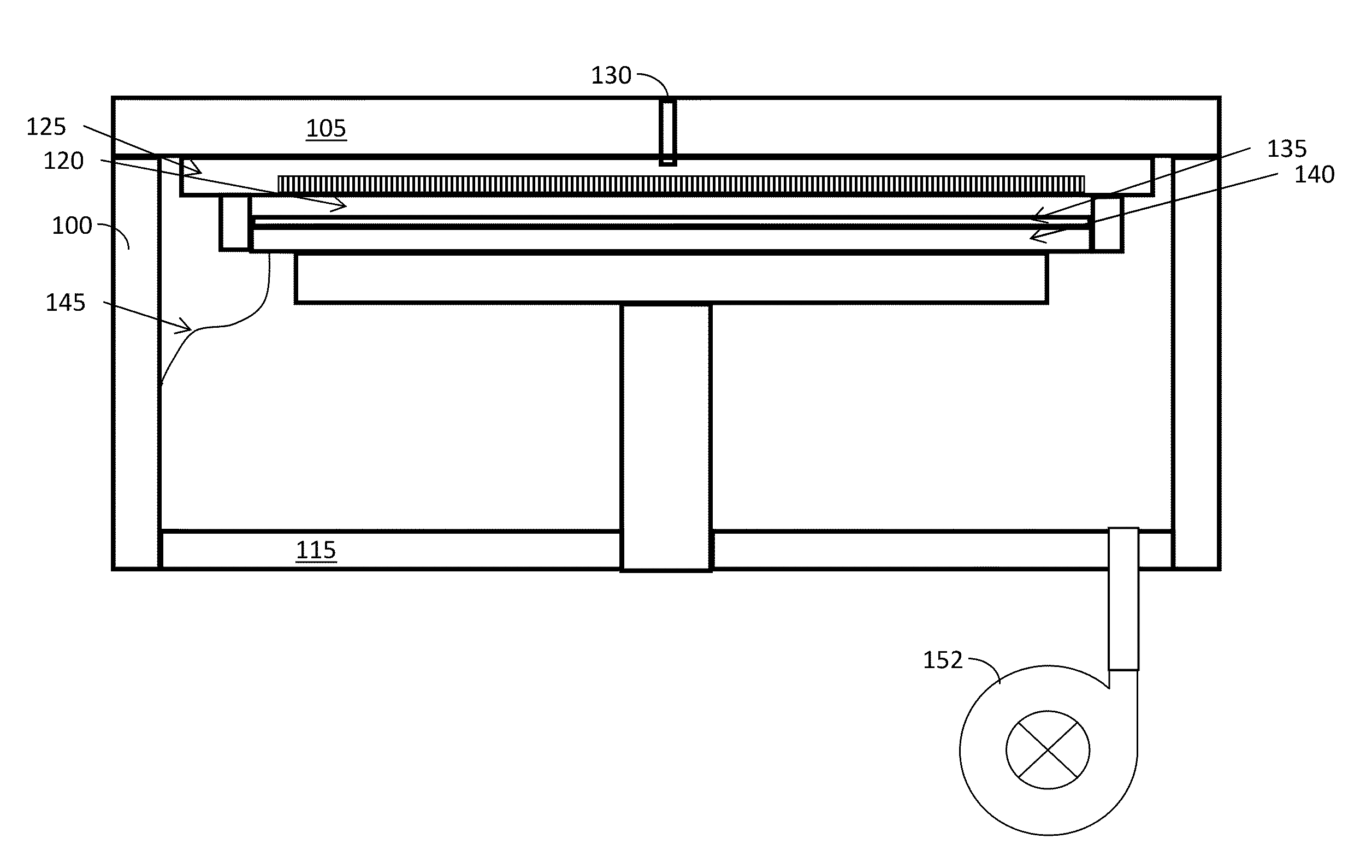
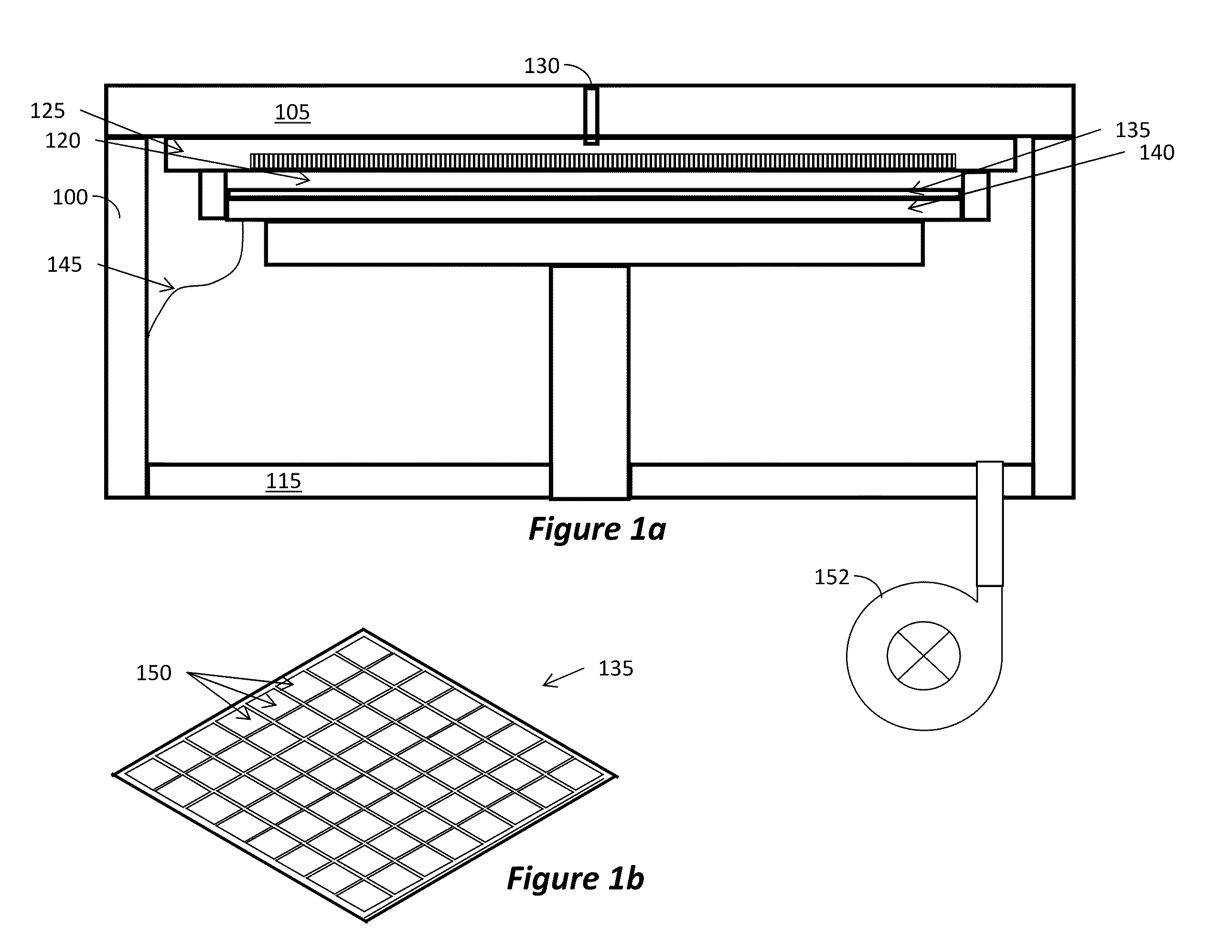
Susceptor for plasma processing chamber
- Summary
- Abstract
- Description
- Claims
- Application Information
AI Technical Summary
Benefits of technology
Problems solved by technology
Method used
Image

Examples
example
A 5″ n-type c-Si solar cell wafer was selected as monitor wafer. Prior to depositing the anti-reflection layer, the wafer has been processed with double sided surface texture, double sided p-type doping and double sided SiO2 coating. During the anti-reflection layer deposition step, around 800A SiN film is deposited on both sides of wafer, resulting in deep blue color. After double sided silicon nitride deposition, the monitor wafer is measured with Sinton WCT-120 photoconductance lifetime tester. The illumination mode is setup as transient (flash setting 1 / 64). The total saturation current density of emitters (Jo) is indicated from PCID simulation software. The monitor has double sided emitters. So the single side saturation current density of emitter is half of the total Jo from PCID. The monitor wafers were processed with several conditions on graphite susceptors with and without coating. The single side saturation current densities of the emitter are compared in the table 1. The...
PUM
| Property | Measurement | Unit |
|---|---|---|
| Thickness | aaaaa | aaaaa |
| Thickness | aaaaa | aaaaa |
| Dielectric polarization enthalpy | aaaaa | aaaaa |
Abstract
Description
Claims
Application Information