Teramos-terahertz thermal sensor and focal plane array

a thermal sensor and terahertz technology, applied in the field of imaging technology, can solve the problems of increasing the system cost, poor state-of-the-art sensitivity, and possible active imaging, and achieve the effects of improving responsivity, wide frequency range of operation, and reducing nois

Active Publication Date: 2011-12-29
TECHNION RES & DEV FOUND LTD
View PDF5 Cites 49 Cited by
  • Summary
  • Abstract
  • Description
  • Claims
  • Application Information

AI Technical Summary

Benefits of technology

[0046]The novel “tiling” concept of sensing-type building blocks enables the achievement of a wide frequency range of operation, while dealing with the issue of real estate available on a reasonably sized die. The combination of the CMOS-SOI-MEMS technologies allows for straightforward integration of sensors and readout, which enables the realization of the “tiling” concept, which in turn enables the realization of the novel concept of variable effective pixel size, composed of combined reading of several pixels. This variable pixel approach enables the achievement of a wide frequency range of operation while dealing with the issue of the real estate available on a reasonably sized die: A die only slightly larger than 6 cm*6 cm provides an array of 256*256 pixels for 1.5 THz imaging and ˜100*100 pixels ...

Problems solved by technology

According to Table II, low cost imaging should be based on antenna coupled bolometers but the state-of-the-art sensitivity is poor and hence only active imaging is possible.
Cryogenic microbolometers (based on superconductors) may provide good sensitivity but the required temperature of operation is 10K or lower, thus increasing consi...

Method used


Image

  • Teramos-terahertz thermal sensor and focal plane array
  • Teramos-terahertz thermal sensor and focal plane array
  • Teramos-terahertz thermal sensor and focal plane array

Examples


Embodiment Construction

[0070]The principles and operation of a method and an apparatus according to the present invention may be better understood with reference to the drawings and the accompanying description, it being understood that these drawings are given for illustrative purposes only and are not meant to be limiting.

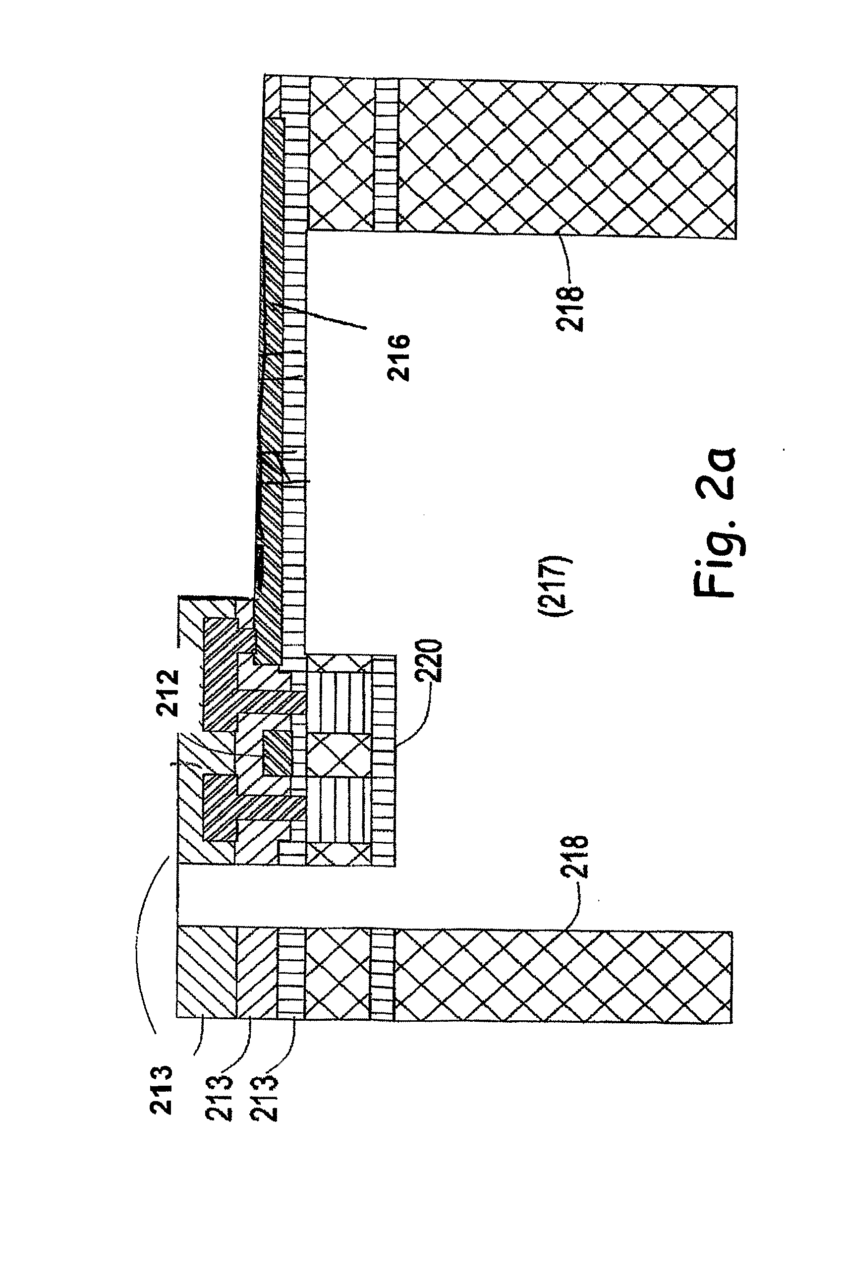
[0071]FIGS. 2a-2c are schematic illustrations of the TeraMOS sensor, constructed according to the principles of the present invention.

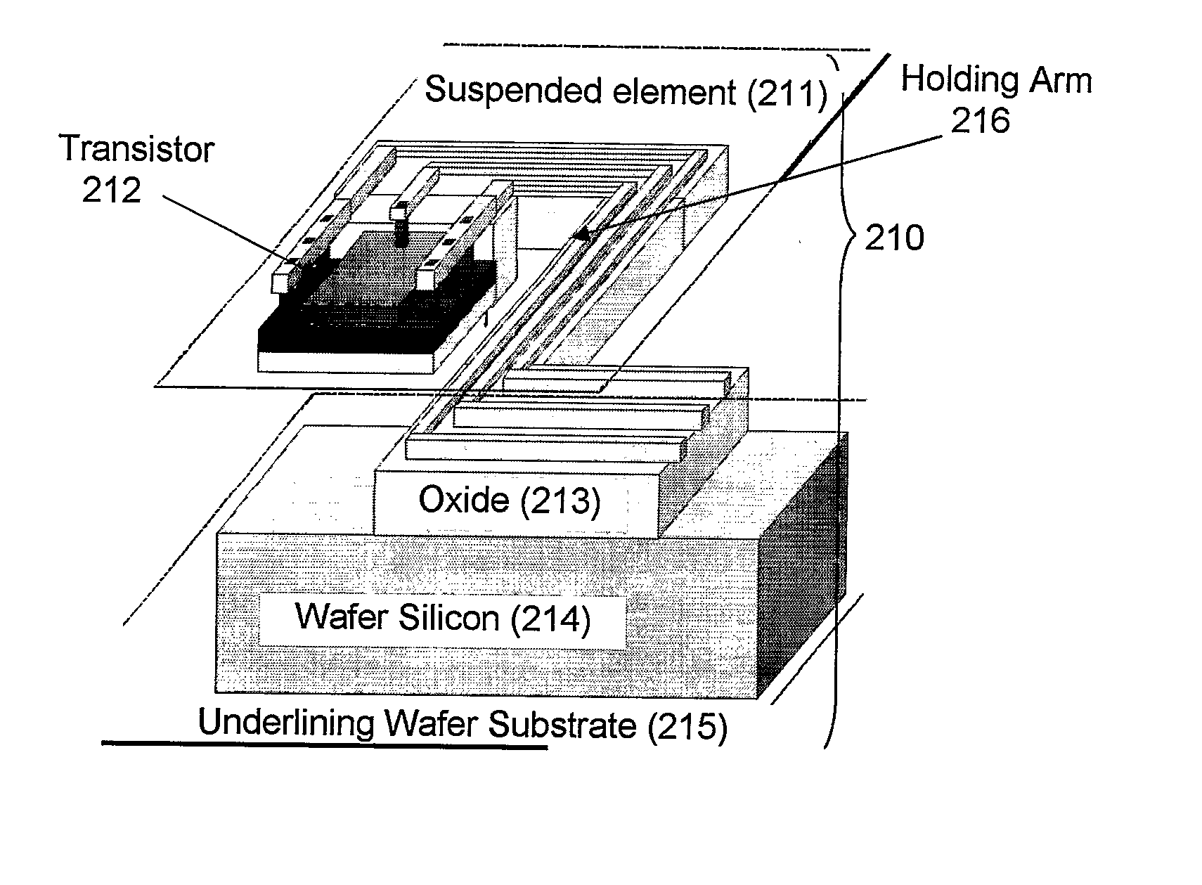
[0072]FIG. 2a is a schematic cross-section of a suspended (released) CMOS transistor 212, held by holding arm 216. The TeraMOS sensor is a thermally isolated micro-machined (released) CMOS transistor, preferably operating at sub-threshold. The schematic cross-section shows the buried oxides 220 along with the additional features of the micro-machined cavity 217 and silicon bulk 218. The CMOS transistor is implemented on an SOI substrate, using Deep Reactive Ion Etch (DRIE) micromachining backside etching, as described in FIG. 9 below.

[0073]The CMOS trans...


PUM


Abstract

A TeraMOS sensor based on a CMOS-SOI-MEMS transistor, thermally isolated by the MEMS post-processing, designed specifically for the detection of THz radiation which may be directly integrated with the CMOS-SOI readout circuitry, in order to achieve a breakthrough in performance and cost. The TeraMOS sensor provides a low-cost, high performance THz passive or active imaging system (roughly in the range of 0.5-1.5 THz) by combining several leading technologies: Complementary Metal Oxide Semiconductor (CMOS)-Silicon on Insulator (SOI), Micro Electro Mechanical Systems (MEMS) and photonics. An array of TeraMOS sensors, integrated with readout circuitry and driving and supporting circuitry provides a monolithic focal plane array or imager. This imager is designed in a commercial CMOS-SOI Fab and the MEMS micromachining is provided as post-processing step in order to reduce cost. Thus the CMOS transistors and technology provide the sensors as well as the signal processing and additional readout circuitry both in the pixels as well as around the sensor array.

Description

FIELD OF THE INVENTION[0001]The present invention relates generally to imaging technology, and more particularly to a method and a system to provide a Focal Plane Array of micro-machined thermally isolated sensors with the supporting and readout circuitry for a low cost, high performance THz passive or active imaging system roughly in the range of 0.5-1.5 THz, by combining three leading technologies: Complementary Metal-Oxide Semiconductor—Silicon on Insulator (CMOS-SOI), Micro Electro Mechanical Systems (MEMS) post-processing and photonics (in the THz radiation range of the electromagnetic spectrum).BACKGROUND OF THE INVENTION[0002]The THz radiation range is usually considered between 0.3-3.0 THz. Within this range, high performance, low-cost passive and or active imaging at 0.5-1.5 terahertz (THz) has well-established benefits, but has been little explored. There is adequate radiation from terrestrial bodies at 300 K to allow passive remote sensing as well as high-resolution image...

Claims


Application Information

Patent Timeline
IPC IPC(8): G01J5/12H01L21/3065H01L29/66
CPCG01J1/4228G01J5/024G01J5/20
Inventor NEMIROVSKY, YAEL
Owner TECHNION RES & DEV FOUND LTD
Why Eureka
Try Eureka