Method for manufacturing thin film capacitor and thin film capacitor obtained by the same

a technology of thin film capacitor and manufacturing method, which is applied in the direction of thin/thick film capacitor, fixed capacitor, material nanotechnology, etc., can solve the problems of deterioration of minute cracking or bubbling of dielectric thin film, and leakage current characteristics, so as to suppress hillocks, superior leakage current characteristics and dielectric breakdown voltage characteristics, the effect of superior leakage current characteristics

Active Publication Date: 2012-01-05
MITSUBISHI MATERIALS CORP +1
View PDF3 Cites 6 Cited by
  • Summary
  • Abstract
  • Description
  • Claims
  • Application Information

AI Technical Summary

Benefits of technology

[0012]It is therefore an object of the present invention to provide a method for manufacturing a thin film capacitor having superior leakage current characteristics and dielectric breakdown voltage characteristics by also removing the cause of hillock generation in processes other than the deposition process for the dielectric thin film and which suppresses hillocks by controlling conditions during such processes.
[0013]It is a further purpose of the present invention to provide a thin film capacitor having superior leakage current characteristics and dielectric breakdown voltage characteristics and low generation of hillocks, and an electronic device provided with the thin film capacitor.

Problems solved by technology

However in this area of thin film capacitors, there are outstanding issues regarding problems such as deterioration in dielectric breakdown voltage characteristics and leakage current characteristics which are thought to result from high-temperature calcining during the manufacturing process.
In the above manufacturing process, in particular, the calcining temperature for crystallization during the deposition process of the dielectric thin film reaches a temperature of more than 800° C. As a result, the dielectric thin film undergoes minute cracking or bubbling due to deterioration of the lower electrode or rapid contraction of the film caused by the high-temperature calcining and, as a result, deterioration in dielectric breakdown voltage characteristics and leakage current characteristics result.
Application of the above type of high-temperature heat process includes further disadvantages such as the production of semispherical protrusions of approximately the same size as the thickness of the lower electrode which are termed “hillocks” on the interface between the dielectric thin film and the lower electrode (on the lower electrode side).
These hillocks cause deterioration in dielectric breakdown voltage characteristics and leakage current characteristics in the same manner as cracking or bubbles produced in the dielectric thin film.
When a hillock is produced, the film thickness of the dielectric thin film at that position is extremely thin in comparison to other portions and therefore the film thickness of the dielectric thin film lacks uniformity.
Consequently leakage current also increases between the upper electrode and the lower electrode when forming a capacitor and dielectric breakdown voltage also deteriorates.

Method used


Image

  • Method for manufacturing thin film capacitor and thin film capacitor obtained by the same
  • Method for manufacturing thin film capacitor and thin film capacitor obtained by the same
  • Method for manufacturing thin film capacitor and thin film capacitor obtained by the same

Examples


example 1

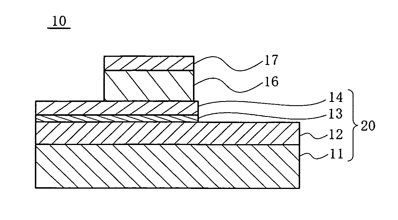
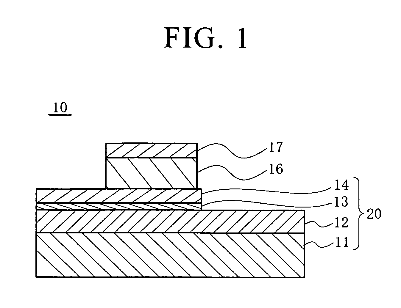
[0049]Firstly as shown in FIG. 1, an insulation film 12 is formed on a substrate 11. More specifically, a SiO2 film having a thickness of 500 nm is formed by thermal processing of a Si substrate having a thickness of 500 μm in an atmosphere of a dried oxidizing gas. Then a metallic Ti film is deposited using a sputtering method on the SiO2 film and subjected to thermal processing for one hour at a temperature of 700° C. to thereby form an adhesion layer 13 having a thickness of 30 nm.

[0050]Then Pt is used as a noble metal in a sputtering method to form a lower electrode 14 having a thickness of 100 nm on the adhesion layer 13. The crystal orientation of the lower electrode 14 displays a preferred orientation with respect to the (111) face. Furthermore the average crystal grain size of the lower electrode 14 is adjusted to be 40 nm. In this manner, the supporting body 20 is formed which includes a substrate 11, an insulation film 12 formed on the substrate 11, and a lower electrode 1...

example 2

[0053]A thin film capacitor was obtained which is the same as the Example 1 except that the dielectric thin film is formed on a lower electrode which has a residual stress value as expressed in Table 1 hereafter and has a thickness of 200 nm. This thin film capacitor will be called Example 2.

example 3

[0054]A thin film capacitor was obtained which is the same as the Example 1 except that the dielectric thin film is formed on the lower electrode which has an average crystal grain size and residual stress as expressed in Table 1 hereafter and has a thickness of 300 nm. This thin film capacitor will be called Example 3.


PUM

PropertyMeasurementUnit
temperatureaaaaaaaaaa

Abstract

A thin film capacitor is characterized by forming a lower electrode, coating a composition onto the lower electrode without applying an annealing process having a temperature of greater than 300° C., drying at a predetermined temperature within a range from ambient temperature to 500° C., and calcining at a predetermined temperature within a range of 500 to 800° C. and higher than a drying temperature. The process from coating to calcining is performed the process from coating to calcining once or at least twice, or the process from coating to drying is performed at least twice, and then calcining is performed once. The thickness of the dielectric thin film formed after the first calcining is 20 to 600 nm. The ratio of the thickness of the lower electrode and the thickness of the dielectric thin film formed after the initial calcining step (thickness of lower electrode/thickness of the dielectric thin film) is preferably in the range 0.10 to 15.0.

Description

BACKGROUND OF THE INVENTION[0001]1. Field of the Invention[0002]The present invention relates to a method for manufacturing a thin film capacitor having superior leakage current characteristics and dielectric breakdown voltage characteristics. More particularly, the present invention relates to a method for manufacturing a thin film capacitor having the superior characteristics above in which formation of hillocks is suppressed during the manufacturing process of the thin film capacitor and which thereby prevents deterioration in dielectric breakdown voltage and increase in leakage current density caused by hillock generation.[0003]2. Description of Related Art[0004]Electronic devices such as a dynamic random access memory (DRAM), a ferroelectric random access memory (FeRAM), an RF circuit or the like are provided with a capacitor. However the demand for higher integration and miniaturizing of devices in recent years has resulted in a corresponding reduction in the area occupied by ...

Claims


Application Information

Patent Timeline
Patent Type & Authority Applications(United States)
IPC IPC(8): H01L29/92H01L21/02
CPCB82Y30/00H01L28/60C04B2235/3213C04B2235/441C04B2235/781C04B2235/785C04B2235/787H01G4/01H01G4/1227H01G4/33H01L21/02197H01L21/02282H01L28/55H01L28/65C04B35/4682
Inventor SAKURAI, HIDEAKIWATANABE, TOSHIAKISOYAMA, NOBUYUKIGUEGAN, GUILLAUME
Owner MITSUBISHI MATERIALS CORP
Why Eureka
Try Eureka