Liquid crystal display device

a liquid crystal display and active matrix technology, applied in the field of active matrix liquid crystal display devices, can solve the problems of color breakage and other problems, and achieve the effect of prolonging the time for holding a voltage applied to a liquid crystal elemen

Active Publication Date: 2012-01-05
SEMICON ENERGY LAB CO LTD
View PDF7 Cites 22 Cited by
  • Summary
  • Abstract
  • Description
  • Claims
  • Application Information

AI Technical Summary

Benefits of technology

[0007]Further, according to the field sequential driving, power consumption of a liquid crystal display device can be reduced as compared to that in the case of using a color filter. However, along with the spread of mobile electronic devices, the degree of demand for lower power consumption of a liquid crystal display device is getting higher and more and more reduction in power consumption is being demanded.
[0023]However, according to one embodiment of the present invention, a transistor whose off-state current is extremely low is used, whereby a period for holding a voltage applied to a liquid crystal element can be prolonged. Therefore, the driving frequency for displaying a still image can be decreased to a frequency lower than the driving frequency for displaying a moving image. Consequently, a liquid crystal display device whose power consumption is low can be achieved.

Problems solved by technology

However, separate perception of images for respective colors without synthesizing them, a so-called color break-up is likely to occur in the FS driving.

Method used


Image

  • Liquid crystal display device
  • Liquid crystal display device
  • Liquid crystal display device

Examples


embodiment 1

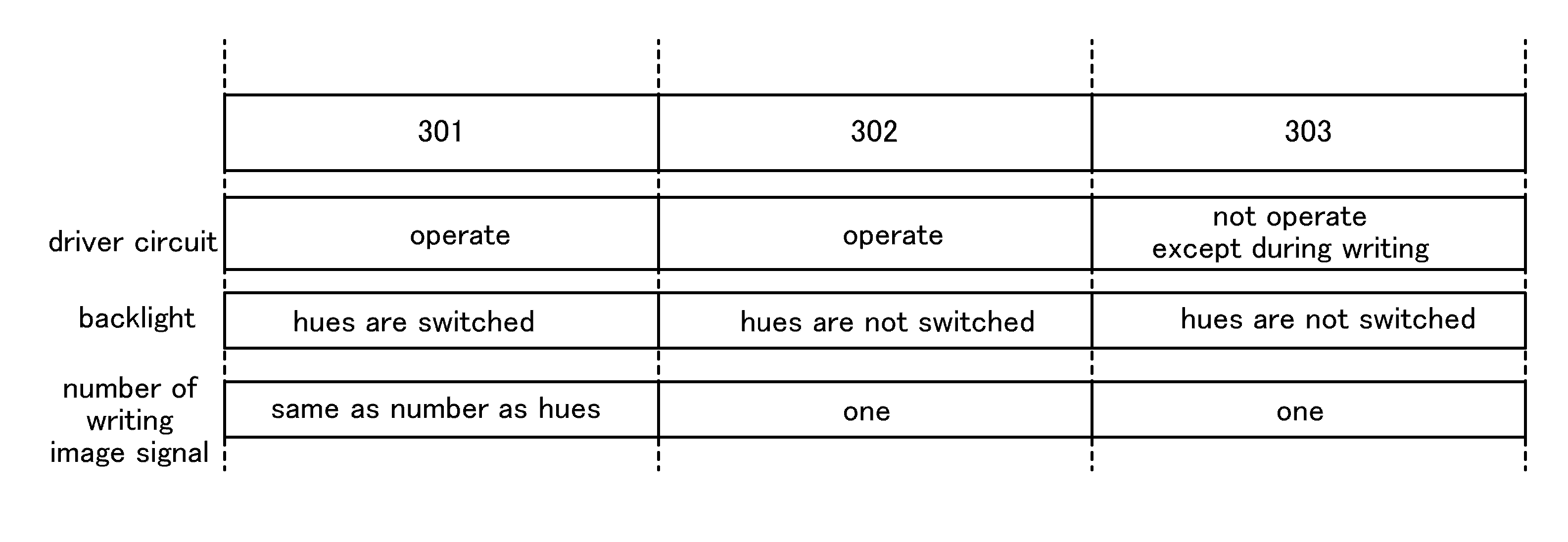
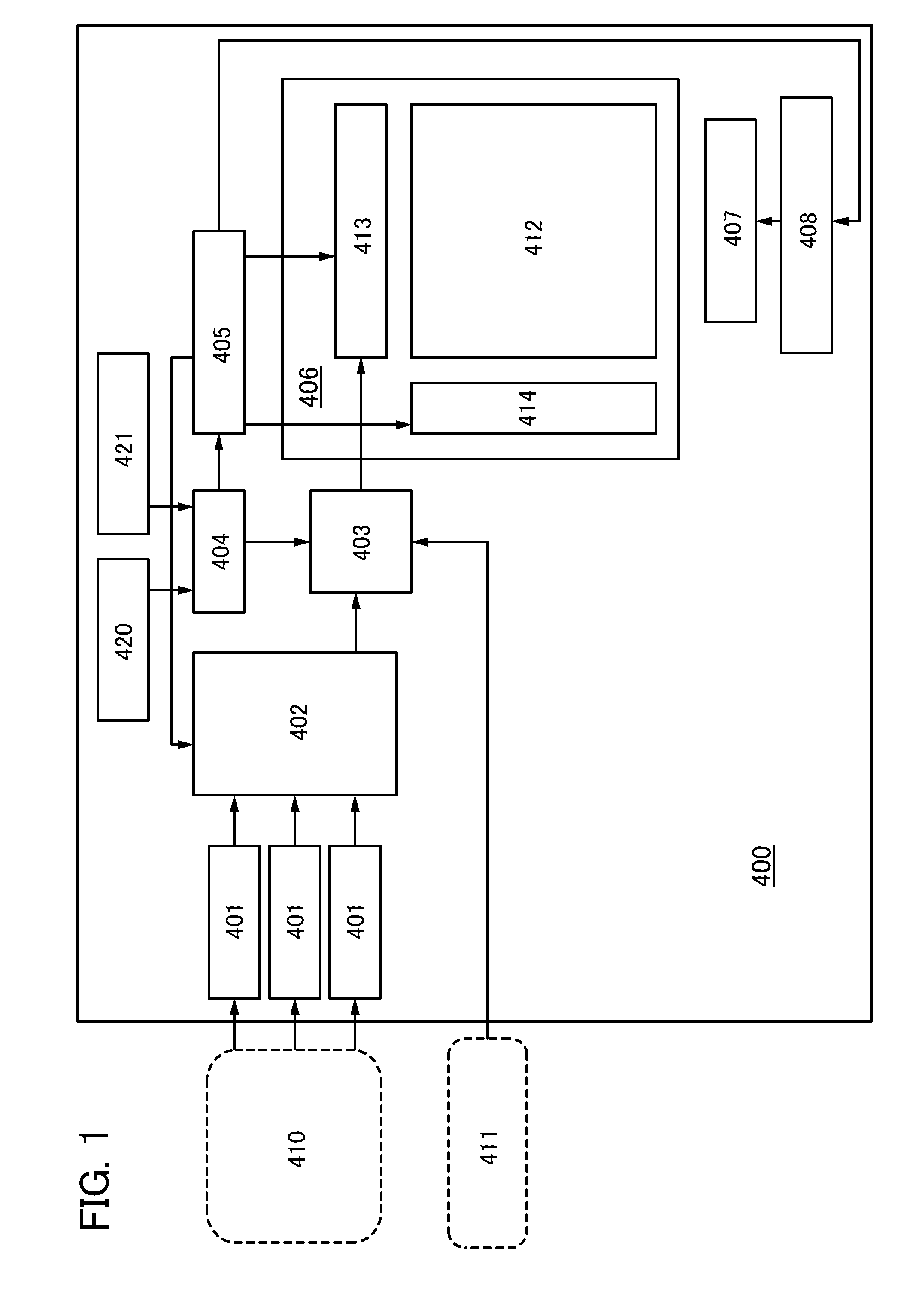
[0057]A liquid crystal display device 400 illustrated in FIG. 1 includes a plurality of image memories 401, an image data selection circuit 402, a selector 403, a CPU 404, a controller 405, a panel 406, a backlight 407, and a backlight control circuit 408.

[0058]Image data for a full-color image (full-color image data 410), which are input to the liquid crystal display device 400, are stored in the plurality of image memories 401. The full-color image data 410 include image data corresponding to their respective hues. The image data corresponding to the respective hues are stored in the respective image memories 401.

[0059]As the image memories 401, for example, memory circuits such as dynamic random access memories (DRAMs) or static random access memories (SRAMs) can be used.

[0060]The image data selection circuit 402 reads the full-color image data, which are stored in the plurality of image memories 401 and correspond to the respective hues, and sends the full-color image data to th...

embodiment 2

[0209]In Embodiment 2, one example of a liquid crystal display device of one embodiment of the present invention, whose panel structure is different from that in Embodiment 1 will be described.

[0210]A specific structure of a panel of one embodiment of the present invention will be described using an example thereof.

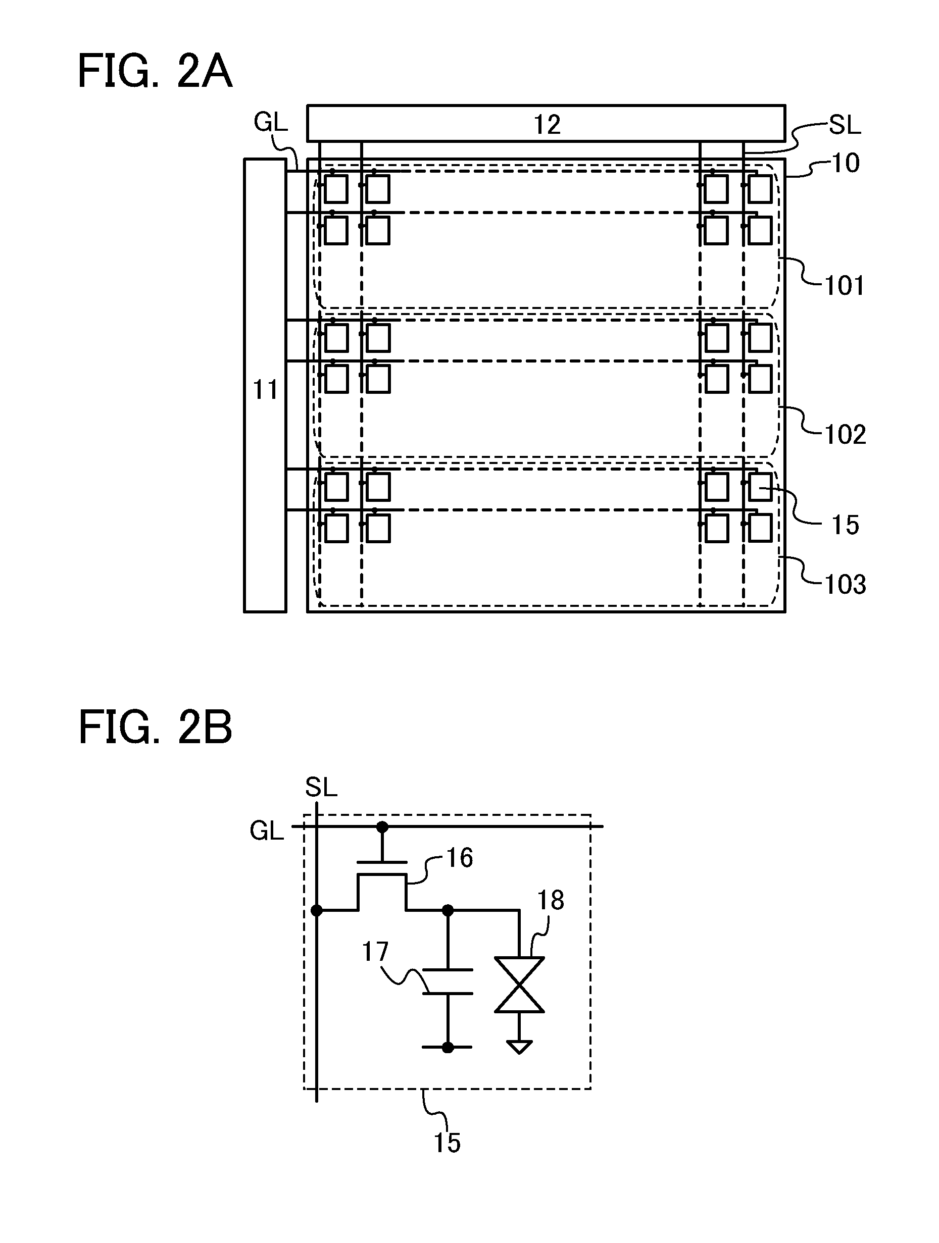
[0211]FIG. 15A illustrates a structural example of a liquid crystal display device. The liquid crystal display device illustrated in FIG. 15A includes a pixel portion 60, a scan line driver circuit 61, and a signal line driver circuit 62. In one embodiment of the present invention, the pixel portion 60 is divided into a plurality of regions. Specifically, the pixel portion 60 is divided into three regions (regions 601 to 603) in FIG. 15A. Each region includes a plurality of pixels 615 arranged in matrix.

[0212]M scan lines GL whose potentials are controlled by the scan line driver circuit 61 and 3×n signal lines SL whose potentials are controlled by the signal line driver ...

embodiment 3

[0248]In Embodiment 3, a manufacturing method of a transistor using an oxide semiconductor will be described.

[0249]First, as illustrated in FIG. 21A, an insulating film 701 is formed over an insulating surface of a substrate 700, and a gate electrode 702 is formed over the insulating film 701.

[0250]Although there is no particular limitation on a substrate which can be used as the substrate 700 as long as it has a light-transmitting property, it is necessary that the substrate have at least enough heat resistance to heat treatment performed later. For example, a glass substrate manufactured by a fusion process or a float process, a quartz substrate, a ceramic substrate, or the like can be used as the substrate 700. In the case where a glass substrate is used and the temperature at which the heat treatment is performed is high, a glass substrate whose strain point is higher than or equal to 730° C. is preferably used. Although a substrate formed of a flexible synthetic resin such as p...


PUM

PropertyMeasurementUnit
off-state currentaaaaaaaaaa
voltageaaaaaaaaaa
voltageaaaaaaaaaa

Abstract

The liquid crystal display device includes a pixel portion including first and second regions and light sources. The first and second regions each include a liquid crystal element whose transmissivity is controlled in accordance with a voltage of an image signal and a transistor for controlling holding of the voltage, whose off-state current is extremely low. The light sources perform first and second drivings: lights whose hues are different from each other are sequentially supplied to the first region in a first rotating order and the lights are sequentially supplied to the second region in a second rotating order which is different from the first rotating order in the first driving; and a light having a single hue is supplied consecutively to one or both of the first and second regions in the second driving. The period for holding the voltage is different between the first and second drivings.

Description

TECHNICAL FIELD[0001]The present invention relates to an active-matrix liquid crystal display device including a transistor in a pixel.BACKGROUND ART[0002]In a transmissive liquid crystal display device, power consumption of a backlight largely affects power consumption of the whole of the liquid crystal display device, and therefore, reduction of light loss within a panel is important for reduction of power consumption. Loss of light within a panel is caused by light refraction in an interlayer insulating film, light absorption in a color filter, or the like. In particular, the light loss is large in principle in a color filter in which light absorption by a pigment is used to extract light having a predetermined range of wavelengths from white light. As a matter of fact, 70% or more of the energy of light from the backlight is absorbed by the color filter. As described above, the color filter hinders reduction in power consumption of the liquid crystal display device.[0003]To avoi...

Claims


Application Information

Patent Timeline
Patent Type & Authority Applications(United States)
IPC IPC(8): G09G3/36G02F1/13357G09G5/10G02F1/1368
CPCG09G3/3413G09G2310/0235G09G3/3688G09G3/3677G02F1/133G02F1/1368G09G3/36
Inventor YAMAZAKI, SHUNPEIKOYAMA, JUNMIYAKE, HIROYUKITOYOTAKA, KOUHEI
Owner SEMICON ENERGY LAB CO LTD
Why Eureka
Try Eureka