Micromachined magnetic field sensors

a magnetic field sensor and micro-machine technology, applied in the field of sensing devices, can solve the problems of large azimuth error of hall sensors constructed by multiple sensors, difficulty in constructing on-chip 3-axis hall sensors required by inability to meet the requirements of low-cost electronic compass applications, etc., to enhance the performance of magnetic field sensors, reduce sensor offset, and increase sensor sensitivity

Active Publication Date: 2012-01-12
INVENSENSE
View PDF5 Cites 69 Cited by
  • Summary
  • Abstract
  • Description
  • Claims
  • Application Information

AI Technical Summary

Benefits of technology

[0009]A micromachined magnetic field sensor integrated with electronics is disclosed. The magnetic field sensors utilize Hall-effect sensing mechanisms to achieve 3-axis sensing by placing Hall sensing elements on the slope sidewall and to increase sensor sensitivity by integrating high mobility layer. A stress isolation structure is proposed to reduce sensor offset. A Z-axis sensor can be fabricated either on a device layer or on a conventional IC substrate with

Problems solved by technology

However, a CMOS Hall sensor features mediocre performance with marginal sensitivity for electronic compass application are often corrupted by sensor offset which is about 1000× larger than the signal generated from the earth magnetic field.
In addition, the thin-film process of CMOS technology is ideal to sense the magnetic field perpendicular to the chip surface (said Z-axis) and it's challenging to construct on-chip 3-axis Hall sensor required by low-cost electronic compass applications.
Electronics compas

Method used


Image

  • Micromachined magnetic field sensors
  • Micromachined magnetic field sensors
  • Micromachined magnetic field sensors

Examples


second embodiment

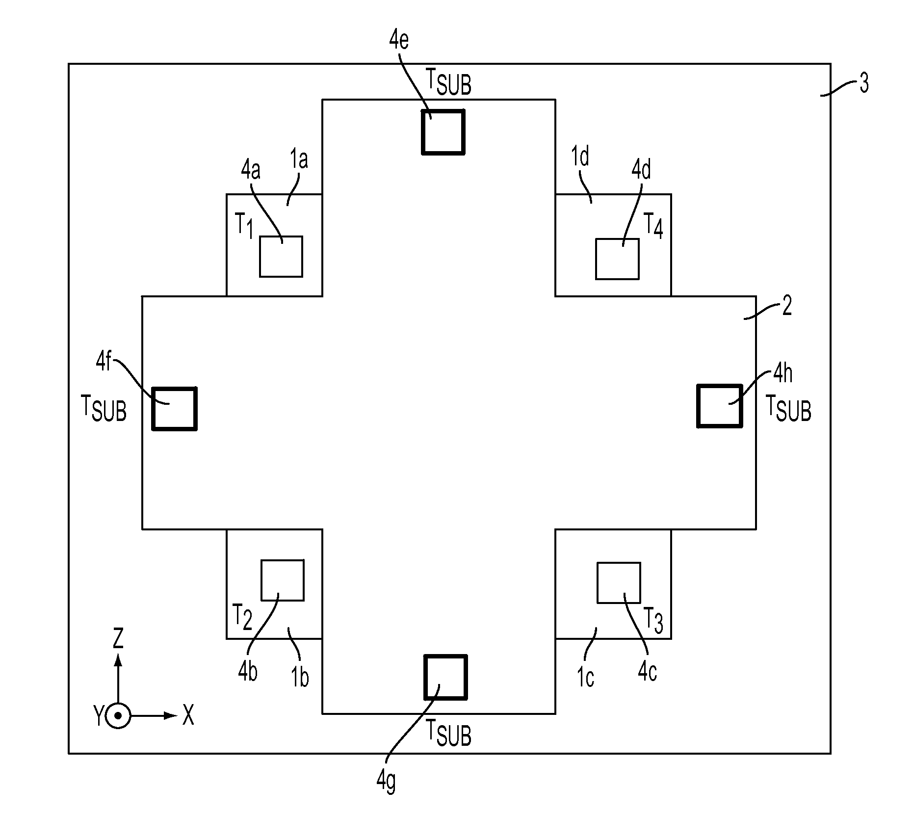
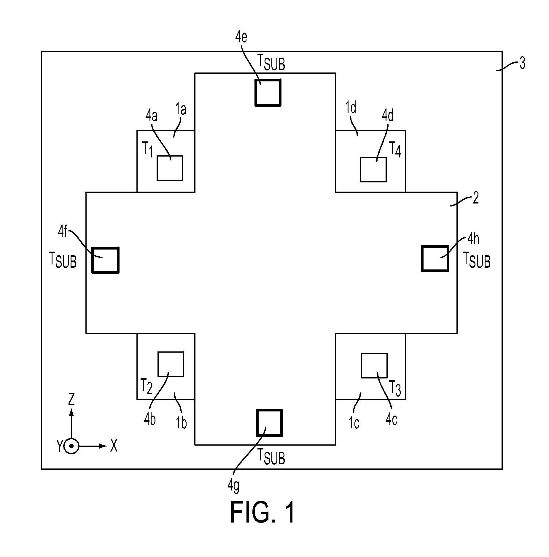
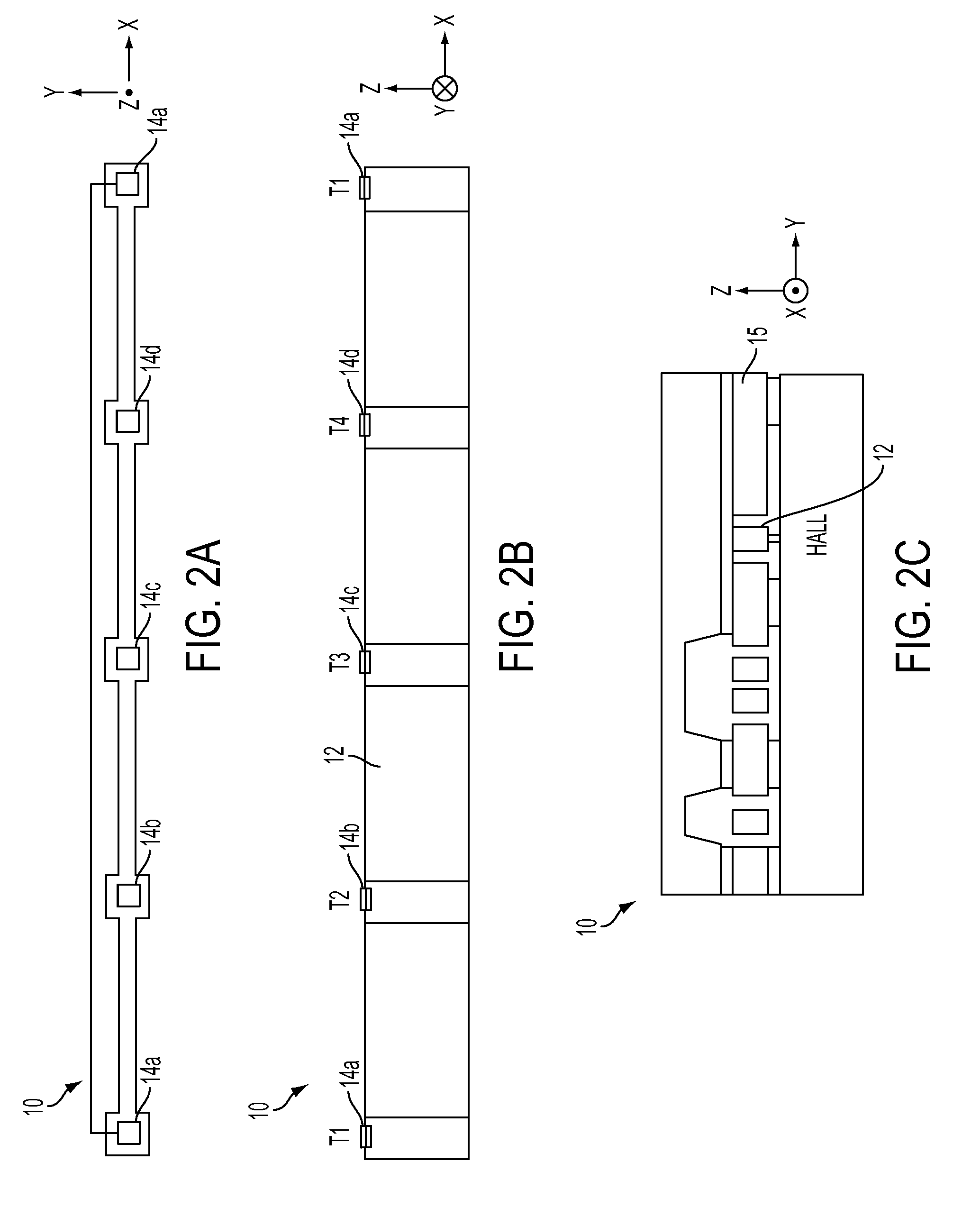
[0037]an X axis or Y axis magnetic field sensor 100 is shown in FIG. 3A-3C. The side-view of a device structure with potential integration with other sensors in the process platform is illustrated in FIG. 3C. The structure has a Hall plate 102 with at least four terminals 104(a)-104(d). The Hall plate 102 is as narrow as a few microns in the Y direction and as deep as the thickness of the device layer in the Z direction. The plate is fabricated on a low-doped single crystal device layer and patterned by DRIE process to form an isolation trench. The device layer is preferred to have N-type doping for its high mobility.

[0038]The electrical terminals 104(a)-104(d) are connected through conductive wiring bridges in the Y direction across the isolation trench, and further connected to the corresponding pads on a conventional IC substrate. To establish the conductive wiring bridges across the isolation trench, a sacrificial layer is deposited followed by the deposition of the conductive w...

third embodiment

[0040]an X axis or Y axis magnetic field sensor 200 is shown in FIG. 4A-4C. The structure has a Hall plate 202 with at least four terminals 204(a)-204(d). The plate is fabricated on a low doped single crystal device layer and patterned by DRIE process to form an isolation trench. The device layer is preferred to have N-type doping for its high mobility.

[0041]T1204(a) and T2204(b) are the source terminals connected to electrical ground and electrical supply such as voltage source or current source, respectively. The remaining two terminals T3204(c) and T4204(d) are the sensing terminals which are connected to voltage sensing circuitry. By supplying the current flowing in Z direction, a Hall voltage between T3 and T4 is generated, which is a function of the magnetic field, and it is sensed by the voltage sensing circuitry. The side-view of a device structure with potential integration with other sensors in the process platform is illustrated in FIG. 4C.

[0042]A fourth embodiment of an ...

fifth embodiment

[0043]an X or Y axis magnetic field sensor 400 is shown in FIG. 6A-6C. The structure and manufacture process is similar to previous embodiments, except for the implementation of a high mobility material 406 deposited on the device layer, orientation of the Hall plate 402 and the arrangement of the sensing terminals.

[0044]T1404(a) and T2404(b) are the source terminals connected to electrical ground and electrical supply such as voltage source or current source, respectively. Near the edge of the isolation trench 403, the current first flows in the negative Z-direction toward the bottom of the device layer, then bends toward the positive Z-direction. The remaining two terminals T3404(c) and T4404(d) are the sensing terminals. The Hall plate 402 is orientated in YZ plane with current flowing in Z direction. Upon applying a magnetic field in X-direction, a Hall voltage between T3404(c) and T4404(d) is generated, is a function of the magnetic field, and is sensed by the sensing circuitry...


PUM


Abstract

A micromachined magnetic field sensor integrated with electronics is disclosed. The magnetic field sensors utilize Hall-effect sensing mechanisms to achieve 3-axis sensing. A Z axis sensor can be fabricated either on a device layer or on a conventional IC substrate with the design of conventional horizontal Hall plates. An X and Y axis sensor are constructed on the device layer. In some embodiments, a magnetic flux concentrator is applied to enhance the performance of the magnetic field sensor. In some embodiments, the magnetic field sensors are placed on slope sidewalls to achieve 3-axis magnetic sensing system. In some embodiments, a stress isolation structure is incorporated to lower the sensor offset. The conventional IC substrate and device layer are connected electrically to form a 3-axis magnetic sensing system. The magnetic field sensor can also be integrated with motion sensors that are constructed in the similar technology.

Description

CROSS-REFERENCE TO RELATED APPLICATIONS[0001]The present application is related to co-pending U.S. patent application, entitled “Micromachined Offset Reduction Structures for Magnetic Field Sensing” Ser. No. ______, filed on even date herewith, and assigned to the assignee of the present invention.FIELD OF THE INVENTION[0002]The present invention relates generally to sensing devices and more specifically to magnetic field sensors.BACKGROUND OF THE INVENTION[0003]Magnetic field sensors are widely deployed in consumer and industrial instruments for applications varying from position sensing, current sensing, data storage, and magnetic compassing. There are many methods to sense magnetic fields including Hall-effect, magneto-diode, magneto-transistor, magnetoresistive-effect, magnetic tunnel junction, magneto-optical, fluxgate, search coil, and Lorentz force-effect.[0004]The Hall effect sensor fabricated by means of CMOS technology is preferred due to its low-cost batch fabrication wit...

Claims


Application Information

Patent Timeline
IPC IPC(8): G01R33/02
CPCG01R33/07G01R33/0011H01L2224/48091H01L2224/73265H01L2924/00014
Inventor LO, CHIUNG C.SEEGER, JOSEPHLIM, MARTIN
Owner INVENSENSE
Why Eureka
Try Eureka