

Semiconductor device
a technology of semiconductors and devices, applied in the direction of semiconductor devices, basic electric elements, electrical appliances, etc., can solve the problems of difficult to freely set threshold voltages and significant reductions in channel mobility, and achieve the effects of suppressing leak current, reducing channel mobility, and high channel mobility
- Summary
- Abstract
- Description
- Claims
- Application Information
AI Technical Summary
Benefits of technology
Problems solved by technology
Method used
Image

Examples
first embodiment
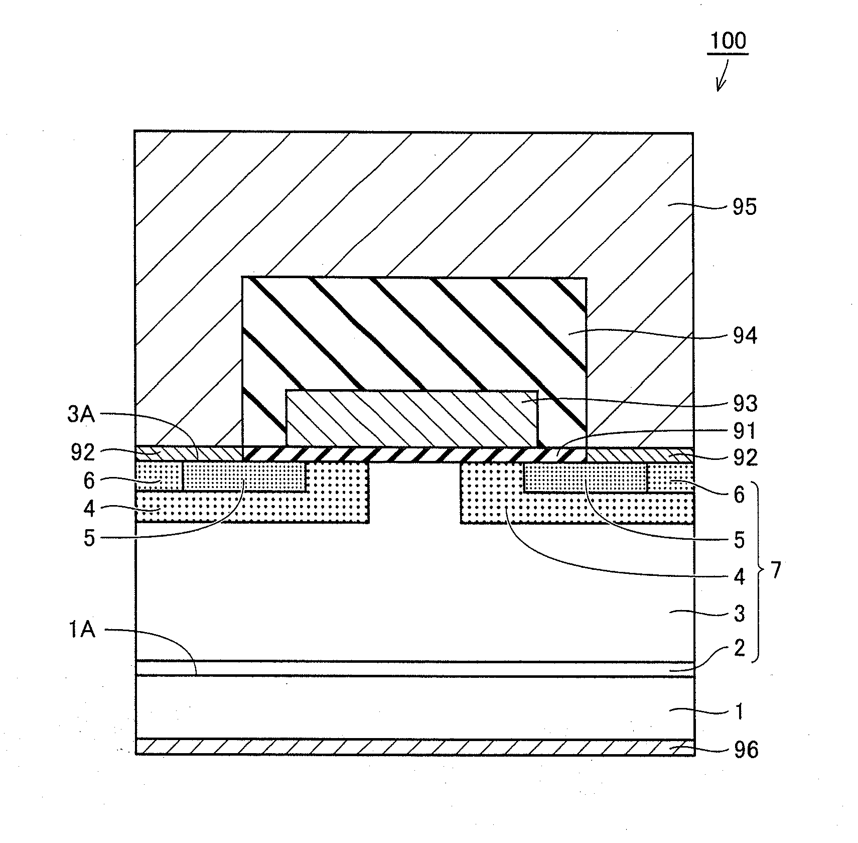
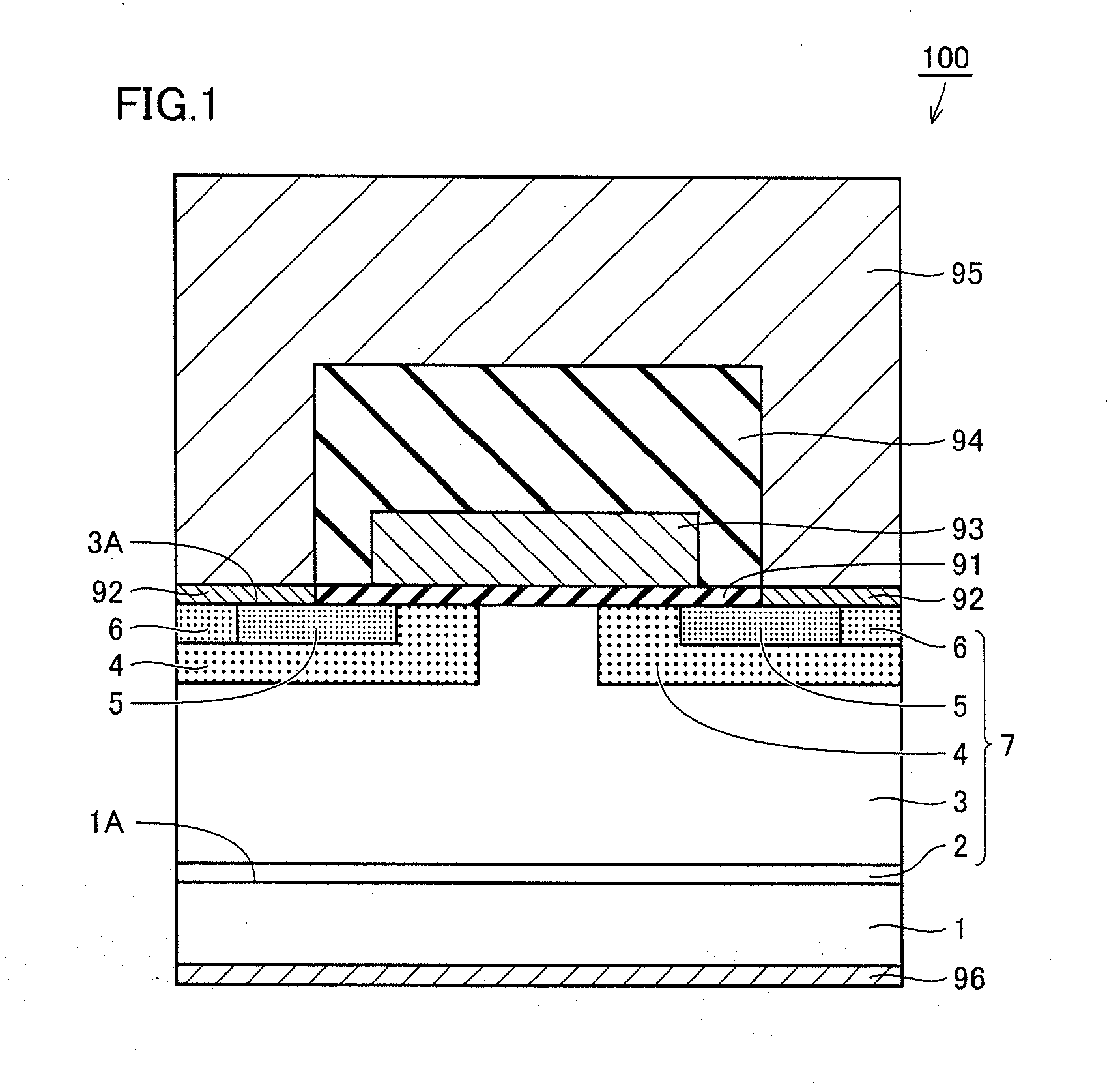
[0064]A first embodiment which is one embodiment of the present invention will be first described. Referring to FIG. 1, a MOSFET 100 which is a semiconductor device (DiMOSFET) in this embodiment includes a silicon carbide substrate 1 of an n conductivity type (first conductivity type), a buffer layer 2 of the n conductivity type made of silicon carbide, a drift layer 3 of the n conductivity type made of silicon carbide, a pair of p type body regions 4 of a p conductivity type (second conductivity type), n+ regions 5 of the n conductivity type, and p+ regions 6 of the p conductivity type.
[0065]Buffer layer 2 is formed on one main surface 1A of silicon carbide substrate 1, and is of the n conductivity type by containing an n type impurity. Drift layer 3 is formed on buffer layer 2, and is of the n conductivity type by containing an n type impurity. The n type impurity contained in drift layer 3 is N (nitrogen), for example, and contained in a concentration (density) lower than that of...
second embodiment
[0108]A second embodiment which is another embodiment of the present invention will now be described. An IGBT 200 which is a semiconductor device in the second embodiment has a similar structure to MOSFET 100 in the first embodiment in terms of plane orientation of the silicon carbide substrate and the p type impurity density in the p type body regions, and thus achieves similar effects.
[0109]Namely, referring to FIG. 7, IGBT 200 which is the semiconductor device in this embodiment includes a silicon carbide substrate 201 of the p conductivity type, a buffer layer 202 (which may be of either the n or p conductivity type), a drift layer 203 of the n conductivity type made of silicon carbide, a pair of p type body regions 204 of the p conductivity type, n+ regions 205 of the n conductivity type, and p+ regions 206 of the p conductivity type.
[0110]Buffer layer 202 is formed on one main surface 201A of silicon carbide substrate 201, and contains an impurity in a concentration higher tha...
first example
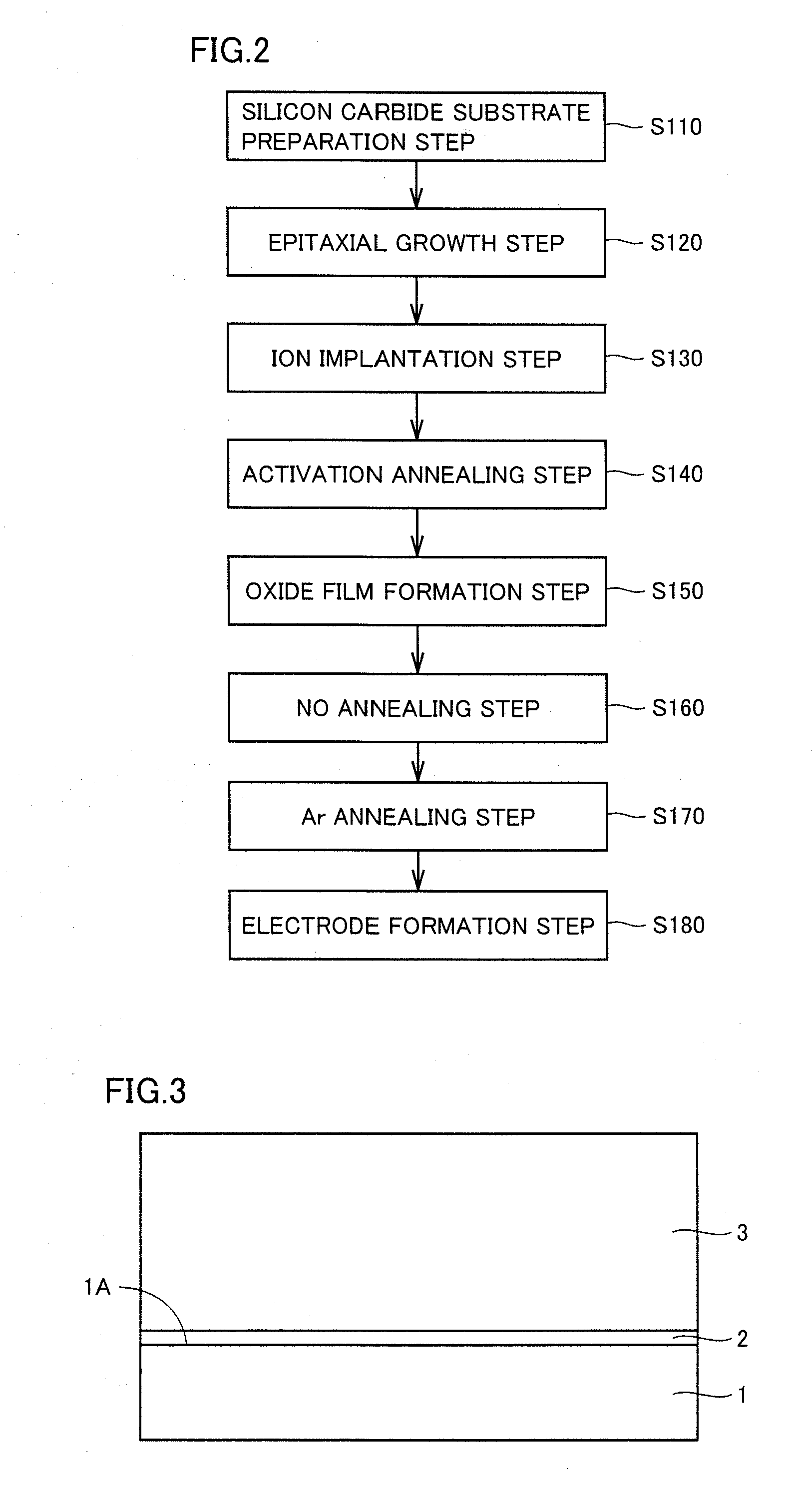
[0129]Experiments were conducted to confirm relation between a doping density of a p type impurity in a p type body region and a threshold voltage. Specifically, first, experimental MOSFETs (samples) were fabricated by a process including a NO annealing step and a Ar annealing step as in the first embodiment. A plurality of samples with different doping densities of a p type impurity in a p type body region were fabricated. Then, a threshold voltage was measured for each sample.
[0130]The experimental results are shown in FIG. 12. In FIG. 12, a horizontal axis represents the doping density of the p type impurity in the p type body region, and a vertical axis represents the threshold voltage. Circles in FIG. 12 are data points obtained from the experiments. A curve in FIG. 12 is a theoretical curve indicating the relation between the doping density and the threshold voltage. The theoretical curve corresponds to an expression (1) indicated below. In the expression (1), ni represents an...
PUM
 Abstract
Description
Claims
Application Information