

Back electrode-type solar cell and method of manufacturing the same
a solar cell and back electrode technology, applied in the field of back electrode-type solar cells, can solve problems such as shadow loss due to electrodes, and achieve the effect of increasing reliability and conversion efficiency
- Summary
- Abstract
- Description
- Claims
- Application Information
AI Technical Summary
Benefits of technology
Problems solved by technology
Method used
Image

Examples
first embodiment
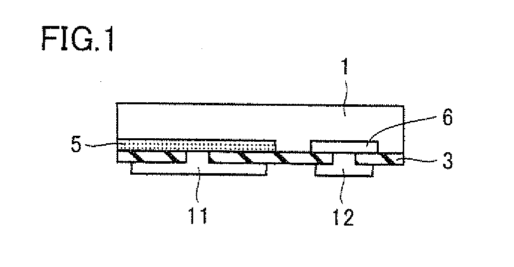
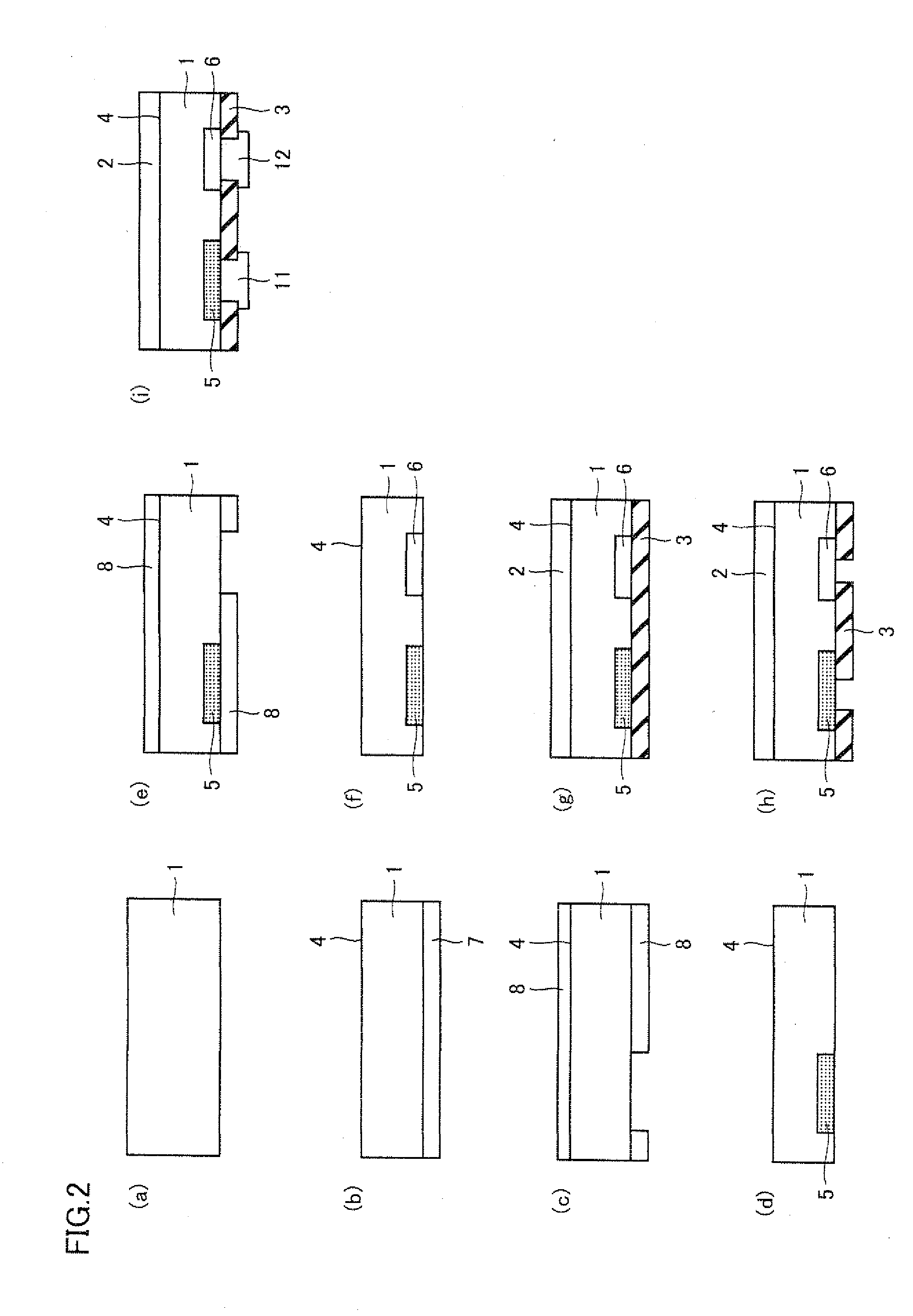
[0023]As shown in FIG. 1, a back electrode-type solar cell of the present invention includes on one surface of a semiconductor substrate 1 of a first conductivity type, a first doped region 6 that is identical in conductivity type to the first conductivity type, and a second doped region 5 of a second conductivity type that is different in conductivity type from the first conductivity type. The back electrode-type solar cell has a first electrode 12 formed on first doped region 6, and a second electrode 11 formed on second doped region 5. When the first conductivity type is a p-type, the second conductivity type is an n-type, and when the first conductivity type is an n type, the second conductivity type is a p-type. First doped region 6 is a region of the first conductivity type, having an impurity concentration higher than that in semiconductor substrate 1, and second doped region 5 is a region having the second conductivity type different from the first conductivity type.
[0024]Wh...
second embodiment
[0051]In connection with the method of manufacturing a back surface contact-type solar cell of the present invention, a method of forming a conductive coating layer using electroless plating as a plating method will be described below. The second embodiment is the same as the first embodiment excluding the plating method, and therefore, the same description will not be repeated.
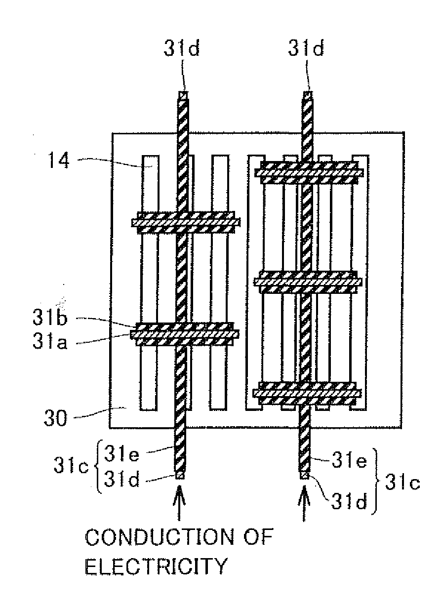
[0052]The step of forming each of the fired electrodes is the same as that in the first embodiment. After forming first electrode 12 and second electrode 11, i.e., fired electrodes, on a back surface of semiconductor substrate 1, semiconductor substrate 1 is immersed in plating solution 15 as shown in. FIG. 4, thereby allowing conductive coating layer 14 to be formed on desired portions.
[0053]First, the semiconductor substrate having the first electrode and the second electrode formed thereon is immersed in an activating agent. An activating agent as exemplified in the first embodiment may be used as an activ...
third embodiment
[0059]In connection with the method of manufacturing a back electrode-type solar cell of the present invention, a method of forming a conductive coating layer by plating utilizing an internal electric field in a solar cell will be described below. The third embodiment is the same as the first embodiment excluding the formation of a conductive coating layer, and therefore, the same description will not be repeated.
[0060]The step of forming each fired electrode is the same as that in the first embodiment. Here, in semiconductor substrate 1, in order to increase the junction area to achieve a high current value, for example, in the case of an n-type semiconductor substrate, a diffusion layer is formed to increase second doped region 5, which is a p+ layer. For example, Japanese Patent Laying-Open No. 2006-332273 (hereinafter denoted as “PTL 3”) describes that the junction area is preferably 60% or more. Generally, making the first and second electrodes identical in width (cross-section...
PUM
| Property | Measurement | Unit |
|---|---|---|
| Electrical conductivity | aaaaa | aaaaa |
| Electrical conductor | aaaaa | aaaaa |
| Electric potential / voltage | aaaaa | aaaaa |
Abstract
Description
Claims
Application Information